Ultra-high precision nano additive manufacturing of metal oxide semiconductors via multi-photon lithography
- Select a language for the TTS:
- UK English Female
- UK English Male
- US English Female
- US English Male
- Australian Female
- Australian Male
- Language selected: (auto detect) - EN
Play all audios:

ABSTRACT As a basic component of the versatile semiconductor devices, metal oxides play a critical role in modern electronic information industry. However, ultra-high precision
nanopatterning of metal oxides often involves multi-step lithography and transfer process, which is time-consuming and costly. Here, we report a strategy, using metal-organic compounds as
solid precursor photoresist for multi-photon lithography and post-sintering, to realize ultra-high precision additive manufacturing of metal oxides. As a result, we gain metal oxides
including ZnO, CuO and ZrO2 with a critical dimension of 35 nm, which sets a benchmark for additive manufacturing of metal oxides. Besides, atomic doping can be easily accomplished by
including the target element in precursor photoresist, and heterogeneous structures can also be created by multiple multi-photon lithography, allowing this strategy to accommodate the
requirements of various semiconductor devices. For instance, we fabricate an ZnO photodetector by the proposed strategy. SIMILAR CONTENT BEING VIEWED BY OTHERS DAMAGE-FREE LED LITHOGRAPHY
FOR ATOMICALLY THIN 2D MATERIAL DEVICES Article Open access 14 February 2023 REMOTE EPITAXIAL CRYSTALLINE PEROVSKITES FOR ULTRAHIGH-RESOLUTION MICRO-LED DISPLAYS Article 15 January 2025
NANOIMPRINT CRYSTALITHOGRAPHY FOR ORGANIC SEMICONDUCTORS Article Open access 16 April 2025 INTRODUCTION Semiconductor chips following Moore’s Law require that lithography technologies evolve
with the times. Although state-of-the-art deep ultraviolet (DUV) and extreme ultraviolet (EUV) lithography enable high-throughput fabrication of nanostructures, expensive masks, and
repetitive exposure transfer are inevitable, which is inaccessible to preliminary scientific exploration1. As an alternative strategy, mask-less multi-photon lithography (MPL) allows the
fabrication of arbitrary 2D/3D nano-architectures and is cheaper, more available, and atomically economical than traditional strategies2,3,4,5, especially in high-precision, small-batch
manufacturing6,7,8,9. However, there are still many challenges to overcome for MPL, and two of the key issues are the undesirable critical dimension (CD) and the scarcity of photoresist
libraries10. To date, most photoresists used for MPL consist of liquid organic polymers that typically have a CD limit of 80–100 nm and struggle to withstand harsh pattern transfer
processes, which can be fatal for chips and device applications11,12. In response, some scientific pioneers have changed their minds by developing precursor photoresists and directly
realizing nano-additive manufacturing of target semiconductors and other functional materials based on MPL13,14,15,16,17. As a result, complex transfer processes can be completely
eliminated. Among them, metal–oxide semiconductors (MOS) have received considerable attention since they are widely used in the next generation of microelectronic devices, including
transistors18, memristors19, optoelectronics20, and sensors21. Precursor photoresists are critical for additive manufacturing of MOS via lithography techniques. Typically, precursor
photoresists for MOS can be divided into three types. The first type is the metal oxide precursor, in which the metal oxide nanoparticles are simply mixed with active resins, and the target
MOS can be achieved by MPL and sintering. At this point, the inhomogeneous size of the nanoparticles and their aggregation in the active resin will lead to defects in the MOS pattern15,22.
Meanwhile, nanoparticles will cause significant light scattering and micro-explosion, giving rise to worse CD and line edge roughness. The second type is metal ion precursors. To solve the
above problems, another strategy is to mix metal ions in the active resins and pyrolyze it after MPL to form MOS patterns23,24. However, this brings new disadvantages. One of them is the low
metal ion content, as they have finite solubility in organic resins (or hydrogel resins) and are lost during the development process, resulting in high shrinkage and poor pattern
quality25,26. More importantly, metal ions, especially transition metal ions, tend to have redox capabilities and could quench active free radicals, thus weakening or even terminating the
polymerization in MPL. The third type is metal-organic compounds (MOCs). MOCs seem to bypass the above shortcomings as they can be blended with a wide range of reactive resins at the
molecular level with sizable loadings. Recently, Bauer et al. reported the fabrication of high-quality fused silica glass nanostructures from polyhedral oligomeric silsesquioxane (POSS)
resin via MPL27. Meanwhile, Xiong et al. introduced metal–organic frameworks into active resins and successfully realized the MPL of 3D MOS, including ZnO and Co3O428. Besides, Malinauskas
et al. employed hybrid organic-inorganic material SZ2080 in MPL to achieve Zr/Si oxides29. Unfortunately, the above MOS precursor photoresists are still in liquid form, which is more
suitable for the construction of 3D nanostructures but difficult to realize ultra-high resolution MOS patterns via MPL. Due to the high migration velocity of free radicals hindering the
possibility of CD improvement30,31, the resulting CD is hardly less than 60 nm32, thus failing to meet the requirements of highly integrated chips and devices. In general, the migration
velocity of free radicals decreases as the shear viscosity increases33,34,35. In addition, the photoresists used in current mature photolithography technologies are all solid films, allowing
for fast, high-resolution, and large-area exposures36,37. Therefore, solid-state precursor photoresists may be more advantageous to form high-resolution MOS patterns. Herein, we report a
universal strategy to achieve multiple MOS patterns with ultra-high precision via MPL by using active MOC-based solid precursor photoresists. Without complex synthesis steps, we chose
commercially available acrylic metal complexes as resins, which can not only form excellent solid films by spin-coating but also highly polymerize by MPL to generate target patterns. To
further suppress the migration of free radicals, a free radical trapping agent (quencher), bis(2,2,6,6-tetramethyl-4-piperidyl-1-oxyl) sebacate (abbreviated as BTPOS), is introduced into the
solid precursor photoresists, by which the excess free radicals will be well confined in a narrower space, thus favoring the improvement of CD38,39. Based on this strategy, typical MOS
including zinc oxide (ZnO), copper oxide (CuO), and zirconium dioxide (ZrO2), are successfully obtained by MPL and subsequent pyrolysis. Remarkably, all three metal oxide patterns have CDs
below 100 nm, with zinc oxide reaching 35 nm, which is comparable to the conventional strategy. Besides, the possibility of atomic doping in MOS pattern is explored by hybriding the trace
element in solid precursor photoresists, Notably, this is very significant for the performance enhancement and application expansion of MOS40,41. Meanwhile, heterostructure MOS patterns are
realized by MPL, proving our strategy can satisfy the additive manufacturing of complex micro-devices. Finally, we fabricate a ZnO photodetector by our strategy. Overall, this work sets a
benchmark for ultra-high precision nano additive manufacturing of metal oxide semiconductors, and may pay the way for MPL toward nano additive manufacturing of highly integrated chips and
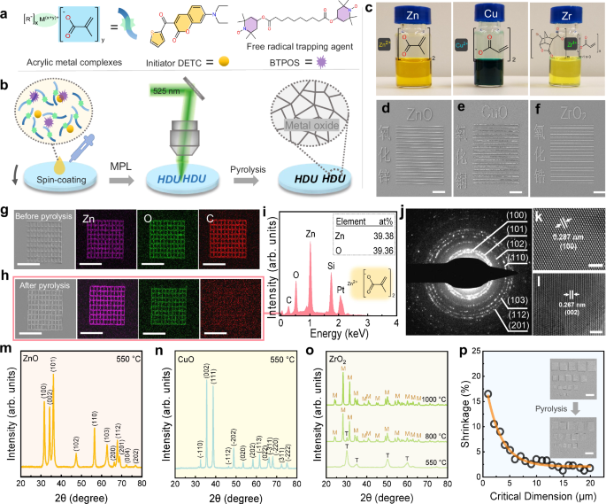
devices. RESULTS PATTERNING METAL OXIDES USING SOLID PRECURSOR PHOTORESISTS As shown in Fig. 1a, the solid precursor photoresists consist of acrylic metal complexes, initiator (DETC), and
free radical trapping agent (BTPOS). Figure 1b shows the step-by-step schematic diagram of the additive manufacturing process of MOS via MPL to prepare the photoresist films, acrylic metal
complexes, initiator, and BTPOS are dissolved in a solvent (Fig. 1c and Supplementary Fig. 1), and then spin-coated on the substrate. Although the resultant photoresist films (approx. 30 nm
in thickness) inherit the color of the metal ions and DETC (Supplementary Fig. 2), they still have good transmittance to the wavelength (525 nm) of the used laser (Supplementary Figs. 3–5),
which can ensure the feasibility of MPL. During the MPL process, DETC in the exposure area can generate a large number of free radicals through multi-photon absorption, which in turn
triggers the polymerization of the carbon-carbon double bonds in the precursor photoresist, leading to a significant solubility difference from the unexposed photoresist, and ultimately the
target pattern is obtained after development. After MPL development, and sintering, the targeted 2D micropatterns are successfully realized using Zn, Cu, and Zr-based acrylic metal
complexes, respectively (Fig. 1d–f). Obviously, the fabricated Chinese characters from Zn/Cu/Zr-based precursor photoresists are highly recognizable, dense, and free of pores. Meanwhile, the
sintering process does not lead to any significant deformation or distortion of the generated line arrays, regardless of the acrylic metal complex used (Fig. 1d–f), indicating that the
present strategy is versatile and potentially capable of realizing high-precision MOS. The composition of the micropatterns is confirmed by energy-dispersive X-ray spectroscopy (EDS),
transmission electron microscope (TEM), and X-ray diffraction (XRD). Prior to sintering, the micropatterns generated by the Zn-based precursor photoresist mainly contain Zn, O, and C
elements (Fig. 1g), while after sintering, it is difficult to recognize the C element (Fig. 1h), suggesting that the organic components are removed during the sintering process. EDS spectrum
(Fig. 1i) shows the atomic percentages of the micropatterns after sintering, the respective atomic ratios of Zn and O are 31.11% and 31.13%, i.e., Zn/O = 1.00, which is consistent with the
atomic ratio of the ZnO crystal. Notably, trace C (atomic ratio: 2.30%) is mainly from combustion residue and SEM sediment contamination23, Si derives from the silicon substrate, and Pt
comes from the sputtered conductive layer on the sample surface. The TEM selected area electron diffraction (SAED) patterns of pyrolyzed Zn-based precursor photoresist (Fig. 1j) exhibit the
characteristic rings of ZnO crystals, and high-resolution transmission electron microscopy (HRTEM) images also provide two typical space lattices (0.287 nm (100), and 0.267 nm (002)) of ZnO
crystals (Fig. 1k, l), proving that the main component after sintering should be ZnO. In addition, all the sharp diffraction peaks observed from the XRD spectra of Fig. 1m are in good
agreement with the standard polycrystalline zinc oxide card (JCPDS No. 36-1451), and no other peaks (such as the graphitized carbon at 26°) are observed, indicating that no by-products or
impurities are generated, and the final micropatterns are composed of ZnO. Likewise, using Cu or Zr-based precursor photoresist, the successful additive manufacturing of CuO and ZrO2
micropatterns is confirmed by EDS (Supplementary Figs. 6 and 7) and XRD (Fig. 1n, o). As shown in Fig. 1n, all the sharp diffraction peaks observed are consistent with standard
polycrystalline CuO card (JCPDS No. 45-0937), and no other peaks are observed, which indicate that the product is polycrystalline CuO. Unlike ZnO and CuO, the crystalline form of ZrO2
depends on the sintering temperature (Fig. 1o), and at 550 °C the tetragonal phase (JCPDS No. 49-1642) is predominant. As the sintering temperature increases to 800 °C, the tetragonal phase
gradually transforms into a monoclinic phase (JCPDS No. 37-1484), and finally to a completely monoclinic phase at 1000 °C42,43. Overall, this strategy enables the realization of MOS
micropatterns, including ZnO, CuO, and ZrO2. In general, MOS micropatterns will suffer from structural shrinkage due to the removal of organic components during the pyrolysis process. This
shrinkage is often random and uncontrollable in the previous works23,28, which can be fatal to the design and processing of nanodevices. Therefore, it is crucial to predict or quantify the
sintering shrinkage of MOS patterns. Since ZnO micropatterns have more application scenarios, we quantitatively investigate its pyrolysis shrinkage. As shown in Supplementary Fig. 8, we
fabricate rectangular blocks and parallel lines. It is found that ZnO micropatterns with different line widths have different shrinkage rates. For large rectangular (2.80 μm × 2.85 μm)
patterns, the shrinkage rate after sintering is around 6% in both x and y directions. Interestingly, the absolute value of the shrinkage seems to stay between 200 and 300 nm even though the
side length of rectangular patterns is increased from 5 to 20 µm. This should result from the anchoring effect of the substrate that resists the in-plane shrinkage (parallel to the
substrate) of ZnO micropatterns, and significant shrinkage occurs only in the edge regions that lack sufficient anchoring effect. In view of this, when size decreases, shrinkage is
undoubtedly increased dramatically (Fig. 1p). Typically, the shrinkage rate is as high as 16% (433 nm after sintering) for fine parallel lines with a line width of 516 nm (Supplementary Fig.
8). At sizes below 1 µm, the shrinkage no longer seems to be size-dependent and varies in the range of 12–20%. (Supplementary Fig. 9). It is worth noting that shrinkage rates of MOS
micropatterns reported in the previous literature on MOS are generally as high as 50–70%23,28. In contrast, we offer a strategy that has the distinct advantage of more realistically
reproducing the original design structure without the need for extensive compensation. The high metal content in precursor photoresist is responsible for the ability of our strategy to
fabricate high-fidelity and low-shrinkage MOS micropatterns. As shown in Supplementary Table 1, the precursor photoresist film is almost entirely composed of acrylic metal complexes (wt%
> 98%), which contain metal elements up to 15.05–30.59%. Meanwhile, metal ions will not be washed out during the development process since they are bound to the polymer network through
coordination bonds. Intersecting microstructures in devices is unavoidable and may lead to more defects due to stress anisotropy during shrinkage. As shown in Supplementary Fig. 10, thanks
to the low shrinkage rate of our strategy, the anisotropic shrinkage does not give rise to the fracture and destruction of the grid MOS (ZnO), demonstrating the high fidelity of our
strategy. ULTRA-HIGH PRECISION NANO FABRICATION OF METAL OXIDES As the integration degree of microelectronic devices continues to increase, the requirements for the CD of MOS have also
risen. Although MPL can exceed the diffraction limit and achieve a feature size of nearly 100 nm with the aid of nonlinear absorption, the migration of free radicals hinders the further
improvement of precision. In addition to utilizing solid-state precursor photoresists to reduce free radical migration, we further introduce free radical trapping agent (Fig. 1a, BTPOS) into
photoresists, whereby free radicals can be confined to a very small space (Fig. 2a), and thus facilitates ultra-high-precision additive manufacturing. As shown in Fig. 2b–d, at a fixed
scanning speed of 1000 μm s−1, the line widths of all three oxides, CuO, ZrO2, and ZnO, become progressively smaller as the laser power decreases until they cannot be retained in the
development process. It should be noted that the scatter data in Fig. 2b–d tend to be more linear than those reported in the literature44,45,46, which may be due to the introduction of BTPOS
and the sintering shrinkage. Specifically, the CD of CuO lines is 36 nm, and better surface morphology can be obtained at 52 nm (Fig. 2b). For ZrO2, CD can only reach 58 nm and high-quality
lines are achieved at 72 nm (Fig. 2c). Remarkably, high-quality ZnO line arrays are consistently realized at line-width of 54 nm (Fig. 2e) and even 35 nm (Fig. 2f). Apparently, Zn-based
acrylic metal complexes enable the highest additive manufacturing precision for ZnO, after all, all precursor photoresists use the same initiator, radical trapping agent, and ratios.
However, the underlying principles seem unclear, so we will look into it next. It is believed that CD depends on the nonlinearity absorption exponent (_N)_ of the photoresist, apart from
wavelength (_λ_), numerical aperture (NA), and technical factor (_k_)47,48,49,50,51. Wegener’s team discussed the resolution of DLW in detail in their work, which we refer to here52.
According to the usual Fraunhofer diffraction formula of a grating, we can derive the Abbe condition. As shown in Fig. 2g, assume a single parallel exposure to the photoresist, forming a
grating with critical period _a__xy_. With a laser wavelength of 525 nm and an NA value of 1.45 for the objective lens, we can determine an _a__xy_ of 181 nm. To determine the exposure dose,
we can assume that the local exposure dose is simply proportional to the density of molecules excited by light absorption. For one-photon absorption, the exposure dose is proportional to
the light intensity at a fixed exposure time. For two-photon (three-photon) absorption, the exposure dose is proportional to the square (cube) of the light intensity at a fixed exposure
time. It can be obviously seen that the larger the nonlinear absorption exponent is, the smaller the full width at half maximum (FWHM) of the exposure dose is (the minimum achievable line
width is about 40% of the FWHM). Put it another way, the larger the _N_, the smaller the CD53. We explore the threshold power (_P_th) of the above three photoresists and then plot a linear
fit between the _P_th and exposure time (_t_exp) through a double-logarithmic representation (Fig. 2h). Nonlinearity absorption exponent _N_ is calculated from the slope of the linear fit
line (_N_ = −1/slope). Clearly, Zn-based precursor photoresist has the highest _N_ (3.76), followed by Cu-based precursor photoresist (_N_ = 3.52) and Zr-based precursor photoresist (_N_ =
2.76), which leads to the order of their CD (ZnO (35 nm) <CuO (36 nm) <ZrO2 (58 nm)) and is consistent with the above theory. Meanwhile, it also can be seen that Zn-/Cu-based precursor
photoresists have strong absorption in the deep UV region (Supplementary Fig. 11), but not for Zr-based precursor photoresists, suggesting Zn-/Cu-based precursor photoresists are more
likely to absorb the femtosecond laser through higher-order nonlinearities (bigger _N_) to achieve high-precision. It is generally believed that the _N_ of precursor photoresist is normailly
determined by both the resin (acrylic metal complexes) and the initiator (DETC), and further dominated by the excitation energy and ionization energy of them35,54. From DFT calculations
(Supplementary Table 3), Zn-based acrylic metal complexes show larger excitation/ionization energies and more equivalent photon numbers than the others, making it possible to have a bigger
_N_. Since the excitation energy and ionization energy rely on the molecular structure of acrylic metal complexes. Therefore, it is expected to obtain photoresists with higher _N_ by
changing the central metal ions and ligands of acrylic metal complexes, thus realizing further improvement of CD in the future. Undeniably, the CD of the final MOS should also be related to
the shrinkage of the precursor photoresist during polymerization and sintering. The polymerization shrinkage tends to be proportional to the polymerization crosslink density of the resin.
Zr-based acrylic metal complexes contain inactive groups with large steric hindrances and are unable to achieve high cross-linking densities, while polymerization shrinkage will be further
inhibited by the alicyclic groups in their ligands. In contrast, both Zn and Cu-based acrylic metal complexes have two active sites with small steric hindrance, making them easier to realize
high polymerization crosslink density. In this sense, acrylic metal complexes with more active sites and less steric hindrance are desirable for improving CD. As mentioned above, shrinkage
during sintering is mainly due to organic component removal. The ratio of the initial mass of the acrylic metal complexes to the mass of the final resulting MOS can reflect its shrinkage
potential. As shown in Supplementary Table 1, the order of mass reduction of the three metal composites before and after pyrolysis is Zr > Zn > Cu. It should be noted that a large mass
loss during the pyrolysis is likely to cause more defects and poor quality, and the lines may be broken and cannot be retained during the shrinkage process, so it is not necessarily
conducive to the improvement of CD. Figure 2i and Supplementary Table 3 show the comparison of CD of MOS realized by various additive manufacturing
technologies15,23,25,28,42,55,56,57,58,59,60,61,62,63,64,65. It is clear that the performance of MPL is much better than the other reported additive manufacturing strategies thanks to the
nonlinear absorption, but it still does not exceed 100 nm due to the rapid migration of free radicals in their material system. In contrast, by utilizing solid-state precursor photoresists
in combination with free radical trapping agents, we surpass the optical diffraction limit and achieve an astonishing CD of 35 nm. Not only is this the benchmark for MOS additive
manufacturing, it also seems to exceed the extreme lithography capabilities of all MPL derived technologies, such as STED lithography66,67,68,69. In addition, while extreme ultraviolet
interference lithography (EUV-IL) and electron beam lithography (EBL) can achieve 10 nm or even 5 nm MOS patterns by virtue of their huge advantages in wavelength, they are difficult to
avoid the use of masks or involve complex pattern transfer processes. At the same time, the above two techniques are too expensive for preliminary scientific exploration. Therefore, this
work provides a good alternative for certain high-precision MOS patterning needs. ATOMIC DOPING AND HETEROGENEOUS METAL OXIDES In many cases, atomic doping is often used to modulate the
bandgap of a semiconductor (known as extrinsic semiconductor) to obtain the target characteristics70,71,72. Therefore, we use ZnO as an example to explore the possibility of Al-doping based
on our strategy. Aluminum acrylate is mixed into the photoresist, and the rest of the process remains unchanged. Aluminum acrylate acts as a reactive monomer during the polymerization
process and participates in the construction of a robust polymer network (Supplementary Fig. 12a), ensuring that the Al atoms are not lost during the development process. We fabricate an
Al-doped ZnO pattern and use a variety of methods to characterize the doping effect. As shown in Supplementary Figs. 12b, c, the EDS mapping results indicate that the sintered pattern mainly
contains Zn and O elements, and the Al elements before and after pyrolysis are difficult to recognize due to the low doping amount. Furthermore, the EDS spectrum (Fig. 3a, b) taken from an
internal beam section shows that the atomic percentages of Zn, O, and Al are 30.65 at%, 32.29 at%, and 0.87 at%, respectively, resulting in an Al to Zn ratio of 0.028. The ratio of Al atom
to Zn atom in raw material is about 0.01, and the main reason for the deviation of the results is the inaccuracy of measuring light elements using EDS. Figure 3c shows the HRTEM images of
Al-doped ZnO, the resultant space lattices are 0.285 nm for (100) and 0.265 nm for (002). Compared to the pure ZnO in Fig. 1m, this lattice reduction is clearly due to the doping of Al
atoms, which induces a deformation of the lattice73. Lattice reduction due to Al-doping can also be confirmed by XRD. As can be seen from Supplementary Fig. 13, the Al-doping has no
influence on the number and intensity of diffraction peaks, indicating that no alumina crystals are generated. However, the diffraction peak position of Al-doped ZnO is found to be slightly
shifted to a larger diffraction angle (Fig. 3d), suggesting that the Al atoms reduce the lattice constant of ZnO74. The lattice constant is expected to be shorter when Al atoms are
substituted into the Zn sites since the ionic radius of Al3+ (0.53 Å) is smaller than that of Zn2+ (0.74 Å)75. Therefore, we can conclude that Al has been successfully doped into the ZnO
crystal at the atomic level and sand that other doping might be achieved by a similar strategy. Since many devices are integrated from multiple materials, i.e., heterogeneous structures.
Thus, we attempt the fabrication of heterogeneous MOS based on MPL. As shown in Fig. 3e–g, we design a quick response (QR) code pattern that consists of ZnO (yellow part), CuO (blue part),
and ZrO2 (green part). By repeating coating-exposure-development three times and subsequent pyrolysis, this heterogeneous QR code is successfully realized (Fig. 3h–j). Due to the difference
in refractive index of the three MOS, they exhibit different brightness under the optical microscope. From the SEM image in Supplementary Fig. 14, the clear boundaries of the MOS indicate
that the MOS prepared in the previous step do not affect the additive manufacturing of the subsequent MOS. Figure 3k–m shows the EDS spectrums and the corresponding elemental maps of the QR
code pattern. Among them, the distribution image of Cu is very clear, and the peak of Cu can be accurately distinguished from the EDS spectrum (Fig. 3l). Although the peaks of Zn (1.012 keV)
and Na (1.041 keV, from the substrate) overlap, as do peaks of Zr (2.042 keV) and Pt (2.048 keV, from the conductive layer), resulting in a relatively fuzzy distribution image, the patterns
can still be distinguished (Fig. 3k–m). By selective elemental imaging of Zn, Cu, and Zr, a color QR code can be obtained (Fig. 3n). This may provide an alternative strategy for encrypting
information at the micro-scale. In addition to the two-dimensional QR code, a three-layer multi-MOS consisting of ZnO, CuO, and ZrO2 is also successfully implemented (Fig. 3o–p), which means
that this strategy has the potential to achieve the layer-by-layer fabrication of heterogeneous MOS. Meanwhile, our strategy can also be used to fabricate real 3D micro-structures
(Supplementary Fig. 15). In a word, this demonstrates the feasibility of fabricating heterogeneous MOS by the present strategy, thus fulfilling various requirements for semiconductor
devices. In addition, another significant advantage of the provided solid precursor photoresist is that it is compatible with air objectives for large-scale additive manufacturing (LS-AM).
Indeed, LS-AM is the basis for truly widespread applications, a barrier that liquid photoresists have struggled to overcome. Supplementary Fig. 16a–c shows the lines printed using solid
precursor photoresists and an air objective (50×, NA = 0.95). Due to the smaller numerical aperture, the CD is increased over the use of oil objectives but remains below 150 nm. Moreover, a
deterioration in line edge roughness is also observed. One possible reason here is that the light intensity edge gradient of the focused spot of different NA objectives is different. The
intensity gradient of the air objective (NA = 0.95) is smaller than that of the oil objective (NA = 1.45), so the edge roughness of the exposure line worsens. Another reason is the standing
wave effect, which will not only cause a decrease in adhesion of the line edge but also make a difference in the developing environment at the edge of the line. Some small monomers in
photoresist are more fully developed than structures attached to the substrate. Notably, the Zr-based photoresist showed the highest precision, possibly because of its better adhesion to the
silicon surface. Subsequently, a Zr-based photoresist is used for LS-AM, and a 2 cm × 2 cm grating with a line width of 190 nm and a resolution of 500 nm is achieved on silicon
(Supplementary Fig. 16d, e). It should be noted that the performance of LS-AM is closely related to the stability of the MPL system, including the stability of the laser power and the
consistency of the focal plane position. We only make a simple demonstration here to illustrate the applicability of the solid precursor photoresist we developed for LS-AM. There are still
many technical issues in practical application, as well as improvements to the formulation of photoresist. PHOTODETECTORS FABRICATION AND PERFORMANCE IMPROVEMENT ZnO is of great value in UV
sensing with a wide direct band-gap (3.37 eV) and large exciton binding energy (≈60 meV) at room temperature76,77, and its UV sensing mechanism is depicted in Supplementary Figs. 17 and 18.
We manufactured some UV photodetectors based on pure ZnO and Al-doped ZnO through our strategy. A schematic diagram of the fabrication process of the UV photodetectors is given in Fig. 4a,
and the as-prepared photodetector unit is shown in Fig. 4b. Under 365 nm irradiation (0.8 mW cm−2), the decay time (the time interval between 90% and 10% of the maximum current value) of ZnO
UV photodetector is 62 s with good photo-cycle stability (Fig. 4c), and the photo-to-dark current ratio (PDCR) is up to 10,500 at an external bias of 3.0 V (Supplementary Fig. 19a). In case
of Al-doped ZnO UV photodetector, the decay time is reduced to 24 s and the PDCR is significantly increased to 16,000 which proves the effectiveness of Al doping (Supplementary Fig. 19b,
c). The performance improvement after Al doping is mainly attributed to the generation of more excited electrons and the edge effect78,79. Meanwhile, the response current of the ZnO
photodetector increases linearly with irradiation intensity for both 365 nm and 254 nm (Fig. 4d and Supplementary Fig. 19d), which means that the fabricated ZnO UV photodetector can be used
to measure the UV intensity of a certain wavelength after calibration. Besides, the fabricated ZnO UV photodetector seems to be more sensitive to 254 nm, e.g., a photo-to-dark current ratio
of up to approx 100,000 (Fig. 4e), which greatly exceeds that of 365 nm (6,500). The photon energy of 365 nm UV light is 3.40 eV, which is close to the bandgap of ZnO (3.37 eV). Due to the
non-zero spectrum width, there still exist photons with energies below the band gap, which cannot generate electron–hole pairs. The photon energy of 254 nm ultraviolet light is 4.88 eV,
which is much higher than the band gap of zinc oxide, and can easily excite electrons to the conduction band, which is why the ZnO UV detector is more sensitive to 254 nm ultraviolet light.
Notably, the superior performance of our devices can be clearly demonstrated by comparison with similar literature (Supplementary Table 4). Meanwhile, the PDCR of the ZnO UV photodetector
might be further improved by our strategy to reduce the line width of ZnO (Supplementary Fig. 20). Subsequently, a 10 × 10 array of ZnO photodetector is further fabricated on a 1-in.
oxidized wafer (Supplementary Fig. 21) to evaluate its potential for UV imaging. The imaging system is illustrated in Fig. 4f, the ZnO UV photodetector array acts as the sensing units, and a
photo-mask with the hollowed pattern ZJ is used to block the light source (365 nm), where the response current of ZnO UV photodetector units is measured at 5.0 V bias. As shown in Fig. 4g,
the response current values between the exposed unit and the shaded unit differ significantly, resulting in a high imaging contrast (Fig. 4h) which coincides with the hollowed pattern ZJ on
the photo-mask. Therefore, it can be concluded that the ZnO photodetectors obtained by the presented additive manufacturing strategy have excellent UV sensing and imaging capabilities.
Except for UV sensing, the ZnO semiconductor has many other applications in microelectronics, such as thin-film transistors80, light-emitting devices81, and gas sensing devices82. In
addition, CuO can be used in gas sensors83 and biosensors84, and ZrO2 can be employed in ferroelectric devices85 and piezoelectric devices86. Noted that many other components on the target
device may not be compatible with the sintering temperature of MOS, one alternative is to print components and then assemble them. In conclusion, the proposed strategy for high-precision
additive manufacturing of MOS patterns has enormous potential in the development and manufacture of microdevices. DISCUSSION Here, we report a strategy using metal-organic compounds as solid
precursor photoresists for the MPL, to realize ultra-high precision nano additive manufacturing of metal oxide semiconductors. Through MPL and post-pyrolysis, metal oxide patterns,
including ZnO, CuO, and ZrO2, can be obtained successfully. Thanks to the limitation of radical migration by solid-state photoresists and the quenching effect of radical trapping agents, the
CD of all three metal oxide patterns are below 60 nm, with ZnO reaching a CD of 35 nm, which sets a benchmark for nano additive manufacturing of metal oxides. In addition, we successfully
realize atomic doping in metal oxide patterns by mixing trace elements in solid precursor photoresists, which could be used to modulate the bandgap of a semiconductor to obtain the target
characteristics. Meanwhile, 2D and 3D heterogeneous structures that consist of ZnO, CuO, and ZrO2 can also be created by multiple MPL, allowing this strategy to accommodate the various
requirements of semiconductor devices. Finally, we fabricate some UV photodetectors by MPL based on the pure ZnO and Al-doped ZnO. It is reasonable to speculate that this strategy may be
applicable to the manufacture of other metal oxides. Overall, this work may provide an alternative strategy for nano additive manufacturing of highly integrated chips and devices. METHODS
MATERIALS Zinc methacrylate, Aluminum acrylate, propylene glycol 1-monomethyl ether 2-acetate (PGMEA), 1-methoxy-2-propanol, and isopropanol (IPA) are purchased from Adamas. Copper (II)
acrylate is purchased from Alfa Aesar. Zirconium bromonorbornanelactone carboxylate triacrylate (PRM30) was purchased from Sigma-Aldrich. 7-Diethylamino-3-thenoylcoumarin (DETC) is purchased
from J&K Scientific. Bis (2,2,6,6- tetramethyl-4-piperidyl-1-oxyl) sebacate (BTPOS) is purchased from TCI. Commercial photoresist AZ1505 and MIF developer are supplied by Tansoole. All
chemicals are used without further treatment. PREPARATION OF METAL-BASED PRECURSOR PHOTORESIST For zinc-based precursor photoresist, zinc methacrylate (150 mg) and DETC (3 mg) are dissolved
in PGMEA (3.0 g) and then filtered twice through a 0.22 μm membrane to obtain a clear yellow solution. Then, BTPOS (4.8 mg) was added to the solution and stirred for 60 min to obtain the
zinc-based precursor photoresist. For copper-based precursor photoresist, copper (II) acrylate (250 mg) and DETC (5 mg) are dissolved in PGMEA (5.0 g) and then filtered twice through a 0.22
μm membrane to obtain a blue clarifying solution. Then, BTPOS (8 mg) was added to the solution and stirred for 60 min to obtain the copper-based precursor photoresist. For zirconium-based
precursor photoresist, zirconium bromonorbornanelactone carboxylate triacrylate (250 mg) and DETC (5 mg) are dissolved in PGMEA (5.0 g) and then filtered twice through a 0.22 μm membrane to
obtain a yellow clarifying solution. Then, BTPOS (8 mg) was added to the solution and stirred for 60 min to obtain the zirconium-based photoresist. For aluminum-doped zinc-based precursor
photoresist, dissolving zinc methacrylate (148.5 mg), aluminum acrylate (1.5 mg), and DETC (3 mg) into PGMEA (3.0 g), then filtering twice with 0.22 μm membrane to obtain a yellow clarifying
solution. Then, BTPOS (4.8 mg) was added to the solution and stirred for 60 min to obtain the Al-doped zinc-based precursor photoresist. For 3D fabrication, the content of metal-organic
compounds and initiators in photoresists both increase threefold, while the rest remains unchanged. MULTI-PHOTON LITHOGRAPHY AND DEVELOPMENT For 2D MOS fabrication, three precursor
photoresist films (approx. 30 nm in thickness) are achieved by spin-coating. Specifically, 2 drops of photoresist solution are dropped onto a glass substrate (thickness = 0.17 mm),
accelerating the rotary coater to 500 rpm for 10 s, and then accelerating to 2000 rpm for 60 s. For zirconium-based precursor photoresists, a quartz substrate is used to replace the glass
substrate since the pyrolysis temperature is up to 1000 °C, which exceeds the maximum temperature that glass can tolerate. MPL is performed using a self-built direct laser writing system,
which consists of a femtosecond laser, acousto-optic modulator, beam expander, galvanometer scanner, scan lens, tube lens, objective, mirrors, and piezoelectric stage. A 525 nm femtosecond
laser (pulse width: 150 fs, repetition rate: 80 MHz) is used as an irradiation source, and a 100× oil-immersion objective lens (NA = 1.45) is used to focus the laser beam. For large-scale
additive manufacturing on wafers, an air objective (50×, NA = 0.95) is used. For micro 3D MOS fabrication, the as-prepared photoresist is drop-casted onto a glass substrate and then dried at
50 °C for 2 h. The laser power used is in the range of 2–30 mW, and the scanning speed is varied from 50 μm s−1 to 10,000 μm s−1. After MPL, metal-based precursor photoresists are developed
with PGMEA for 30 s and then rinsed with IPA for 60 s. PYROLYSIS The samples are pyrolyzed in a muffle furnace (MTI KSL-1200X) at ambient pressure in the air at 10 °C min−1 to a set
temperature (ZnO and CuO at 550 °C, and ZrO2 at 550 °C, 800 °C, and 1100 °C, respectively, to explore the transformation of its crystalline phases) for 60 min and then cooled naturally to
room temperature. FABRICATION AND CHARACTERIZATION OF ZNO PHOTODETECTOR UNIT The Zn-based precursor photoresist is spin-coated (500 rpm for 10 s, followed by 2000 rpm for 60 s) onto the
surface-oxidized silicon (with 300 nm SO2 layer). Afterward, a rectangular structure (100 μm × 20 μm) is exposed using MPL (20× air objective) at 25 mW and 2 m s−1. After exposure, the
sample is developed in PGMEA for 30 s and cleaned with IPA for 60 s to remove the unexposed photoresist. Then, the rectangular ZnO samples can be obtained by sintering at 550 °C for 1 h. ITO
(length, width, and thickness are 100 μm, 100 μm, and 100 nm) electrodes are manufactured by MPL and lift-off process. In detail, the commercial photoresist AZ1505 is spin-coated (2000 rpm
for 60 s) onto the above substrate and pre-baked at 90 °C for 60 s. Two squares (100 μm × 100 μm) are exposed at each end of the rectangular ZnO using the alignment technique. The spacing of
the two squares is 40 μm. Then, post-baking AZ1505 at 90 °C for 60 s, followed by developing with MIF developer (60 s) and water (60 s) to remove the exposed photoresist. ITO electrodes are
achieved by sputtering (Denton Vacuum Discovery 635). Finally, the unexposed AZ1505 photoresist is dissolved using acetone to obtain the ZnO UV photodetector unit. The photoelectronic
properties are tested by a probe station and a semiconductor parameter analyzer (Agilent B1500A). FABRICATION AND CHARACTERIZATION OF ZNO IMAGING ARRAY The preparation method and process
parameters of ZnO UV imaging arrays are almost identical to those of the ZnO UV photodetector unit mentioned above. The difference is that the imaging array has 100 photodetector units (10
rows and 10 columns, with a transverse distance of 0.8 mm and a longitudinal spacing of 1.8 mm between the units). The electrodes of the sensing units are led to the edge of the silicon by
ITO wires to facilitate probe testing. ITO wires (10 μm in width) are fabricated by the same method with ITO electrodes. The imaging performance is tested by a probe station and a
semiconductor parameter analyzer (Agilent B1500A). MATERIAL CHARACTERIZATION Samples are observed by a field emission SEM (Zeiss Sigma 300) at 1 kV. EDS maps are generated by a Zeiss Sigma
300 equipped with an Oxford X-Max SDD EDS system at 5 kV. TEM images are obtained by a high-resolution TEM (JEOL JEM-2100 Plus). All measurements are performed via ImageJ software. The XRD
data is collected by a Rigaku miniflex 600 at 40 kV and 15 mA. The diffractograms are performed from 20° to 80° as the structural information is mainly located in this range. Due to the
limitation of sample size, XRD tests are performed on powder materials. The XRD sample is prepared as follows: the photoresist film is polymerized under 365 nm UV light, then a small amount
of powder can be obtained by scraping the film off the substrate, and the process is repeated until enough sample is obtained. REPORTING SUMMARY Further information on research design is
available in the Nature Portfolio Reporting Summary linked to this article. DATA AVAILABILITY All data are presented in the Article and the Supplementary Information. The data are available
from the authors on request. Source data are provided with this paper. REFERENCES * Khan, H. N., Hounshell, D. A. & Fuchs, E. R. H. Science and research policy at the end of Moore’s law.
_Nat. Electron._ 1, 14–21 (2018). Article Google Scholar * Gonzalez‐Hernandez, D., Varapnickas, S., Bertoncini, A., Liberale, C. & Malinauskas, M. Micro‐optics 3D printed via
multi‐photon laser lithography. _Adv. Opt. Mater._ 11, 2201701 (2022). Article Google Scholar * Barner-Kowollik, C. et al. 3D laser micro- and nanoprinting: challenges for chemistry.
_Angew. Chem. Int. Ed._ 56, 15828–15845 (2017). Article CAS Google Scholar * Butkus, A., Skliutas, E., Gailevičius, D. & Malinauskas, M. Femtosecond-laser direct writing 3D
micro/nano-lithography using VIS-light oscillator. _J. Cent. South Univ._ 29, 3270–3276 (2022). Article CAS Google Scholar * Guan, L. et al. Light and matter co-confined multi-photon
lithography. _Nat. Commun._ 15, 2387 (2024). Article ADS CAS PubMed PubMed Central Google Scholar * Ho, C. M. B. et al. Femtosecond-laser-based 3D printing for tissue engineering and
cell biology applications. _ACS Biomater. Sci. Eng._ 3, 2198–2214 (2017). Article CAS PubMed Google Scholar * Lemma, E. D., Spagnolo, B., De-Vittorio, M. & Pisanello, F. Studying
cell mechanobiology in 3D: the two-photon lithography approach. _Trends Biotechnol._ 37, 358–372 (2019). Article CAS PubMed Google Scholar * Vanmol, K. et al. Two-photon direct laser
writing of beam expansion tapers on single-mode optical fibers. _Opt. Laser Technol._ 112, 292–298 (2019). Article ADS Google Scholar * Gissibl, T., Thiele, S., Herkommer, A. &
Giessen, H. Two-photon direct laser writing of ultracompact multi-lens objectives. _Nat. Photonics_ 10, 554–560 (2016). Article ADS CAS Google Scholar * Wang, H. et al. Two‐photon
polymerization lithography for optics and photonics: fundamentals, materials, technologies, and Applications. _Adv. Funct. Mater._ 39, 2214211 (2023). Article Google Scholar * Jaiswal, A.
et al. Two decades of two-photon lithography: materials science perspective for additive manufacturing of 2D/3D nano-microstructures. _iScience_ 26, 106374 (2023). Article ADS CAS PubMed
PubMed Central Google Scholar * O’Halloran, S., Pandit, A., Heise, A. & Kellett, A. Two‐photon polymerization: fundamentals, materials, and chemical modification strategies. _Adv.
Sci._ 10, 2204072 (2023). Article Google Scholar * Shukla, S. et al. Subwavelength direct laser patterning of conductive gold nanostructures by simultaneous photopolymerization and
photoreduction. _ACS Nano_ 5, 1947–1957 (2011). Article CAS PubMed Google Scholar * Blasco, E. et al. Fabrication of conductive 3D gold-containing microstructures via direct laser
writing. _Adv. Mater._ 28, 3592–3595 (2016). Article CAS PubMed Google Scholar * Long, J. et al. Directional assembly of ZnO nanowires via three-dimensional laser direct writing. _Nano
Lett._ 20, 5159–5166 (2020). Article ADS CAS PubMed Google Scholar * Xiong, W. et al. Laser‐directed assembly of aligned carbon nanotubes in three dimensions for multifunctional device
fabrication. _Adv. Mater._ 28, 2002–2009 (2016). Article CAS PubMed Google Scholar * Balčas, G., Malinauskas, M., Farsari, M. & Juodkazis, S. Fabrication of glass-ceramic 3D
micro-optics by combining laser lithography and calcination. _Adv. Funct. Mater._ 33, 2215230 (2023). Article Google Scholar * Yoo, H. et al. A review of phototransistors using metal oxide
semiconductors: research progress and future directions. _Adv. Mater._ 33, 2006091 (2021). Article CAS Google Scholar * Gul, F. Circuit implementation of nano-scale TiO2 memristor using
only metal-oxide-semiconductor transistors. _IEEE Electr. Device Lett._ 40, 643–646 (2019). Article ADS CAS Google Scholar * Yu, X., Marks, T. J. & Facchetti, A. Metal oxides for
optoelectronic applications. _Nat. Mater._ 15, 383–396 (2016). Article ADS CAS PubMed Google Scholar * Dong, Q., Ryu, H. & Lei, Y. Metal oxide based non-enzymatic electrochemical
sensors for glucose detection. _Electrochim. Acta_ 370, 137744 (2021). Article CAS Google Scholar * Liu, Y. et al. Precise assembly and joining of silver nanowires in three dimensions for
highly conductive composite structures. _Int. J. Extrem. Manuf._ 1, 025001 (2019). Article CAS Google Scholar * Yee, D. W., Lifson, M. L., Edwards, B. W. & Greer, J. R. Additive
manufacturing of 3D-architected multifunctional metal oxides. _Adv. Mater._ 31, 1901345 (2019). Article Google Scholar * Luitz, M. et al. High resolution patterning of an organic-inorganic
photoresin for the fabrication of platinum microstructures. _Adv. Mater._ 33, 2101992 (2021). Article CAS PubMed PubMed Central Google Scholar * Yang, L. et al. Laser printed
microelectronics. _Nat. Commun._ 14, 1103 (2023). Article ADS CAS PubMed PubMed Central Google Scholar * Saccone, M. A., Gallivan, R. A., Narita, K., Yee, D. W. & Greer, J. R.
Additive manufacturing of micro-architected metals via hydrogel infusion. _Nature_ 612, 685–690 (2022). Article ADS CAS PubMed PubMed Central Google Scholar * Bauer, J., Crook, C.
& Baldacchini, T. A sinterless, low-temperature route to 3D print nanoscale optical-grade glass. _Science_ 380, 6648 (2023). Article Google Scholar * Liu, J. et al. 3D printing
nano‐architected semiconductors based on versatile and customizable metal‐bound composite photoresins. _Adv. Mater. Technol._ 7, 2101230 (2022). Article CAS Google Scholar *
Gonzalez-Hernandez, D. et al. Laser 3D printing of inorganic free-form micro-optics. _Photonics_ 8, 577 (2021). Article CAS Google Scholar * Zhang, S. et al. High-efficiency two-photon
polymerization initiators based on coumarin derivatives for additive manufacturing with sub-wavelength resolution. _Mater. Today Chem._ 30, 101599 (2023). Article CAS Google Scholar *
Pingali, R. & Saha, S. K. Reaction-diffusion modeling of photopolymerization during femtosecond projection two-photon lithography. _J. Manuf. Sci. Eng._ 144, 021011 (2021). Article
Google Scholar * Merkininkaitė, G., Aleksandravičius, E., Malinauskas, M., Gailevičius, D. & Šakirzanovas, S. Laser additive manufacturing of Si/ZrO2 tunable crystalline phase 3D
nanostructures. _Opto-Electron. Adv._ 5, 210077 (2022). Article Google Scholar * Andrzejewska, E., Podgorska-Golubska, M., Stepniak, I. & Andrzejewski, M. Photoinitiated polymerization
in ionic liquids: kinetics and viscosity effects. _Polymer_ 50, 2040–2047 (2009). Article CAS Google Scholar * Harinarayana, V. & Shin, Y. C. Two-photon lithography for
three-dimensional fabrication in micro/nanoscale regime: a comprehensive review. _Opt. Laser Technol._ 142, 107180 (2021). Article CAS Google Scholar * Yang, L. et al. On the
Schwarzschild effect in 3D two‐photon laser lithography. _Adv. Opt. Mater._ 7, 1901040 (2019). Article CAS Google Scholar * Sanders, D. P. Advances in patterning materials for 193 nm
immersion lithography. _Chem. Rev._ 110, 321–360 (2010). Article CAS PubMed Google Scholar * Lim, G., Lee, K., Choi, S. & Yoon, H. J. Organometallic and coordinative photoresist
materials for EUV lithography and related photolytic mechanisms. _Coord. Chem. Rev._ 493, 215307 (2023). Article CAS Google Scholar * Mayer, F. et al. 3D two-photon microprinting of
nanoporous architectures. _Adv. Mater._ 32, 2002044 (2020). Article ADS CAS Google Scholar * Hahn, V. et al. Two-step absorption instead of two-photon absorption in 3D nanoprinting.
_Nat. Photonics_ 15, 932–938 (2021). Article ADS CAS Google Scholar * Ye, Z., He, H. & Jiang, L. Co-doping: an effective strategy for achieving stable p-type ZnO thin films. _Nano
Energy_ 52, 527–540 (2018). Article CAS Google Scholar * Fortunato, E., Barquinha, P. & Martins, R. Oxide semiconductor thin-film transistors: a review of recent advances. _Adv.
Mater._ 24, 2945–2986 (2012). Article CAS PubMed Google Scholar * Desponds, A. et al. 3D printing and pyrolysis of optical ZrO2 nanostructures by two-photon lithography: reduced
shrinkage and crystallization mediated by nanoparticles seeds. _Small_ 17, 2102486 (2021). Article CAS Google Scholar * Prasad, K., Pinjari, D. V., Pandit, A. B. & Mhaske, S. T.
Synthesis of zirconium dioxide by ultrasound assisted precipitation: effect of calcination temperature. _Ultrason. Sonochem._ 18, 1128–1137 (2011). Article CAS PubMed Google Scholar *
Cao, C. et al. Cellulose derivative for biodegradable and large-scalable 2D nano additive manufacturing. _Addit. Manuf._ 74, 103740 (2023). CAS Google Scholar * Cao, C. et al. Click
chemistry assisted organic-inorganic hybrid photoresist for ultra-fast two-photon lithography. _Addit. Manuf._ 51, 102658 (2022). CAS Google Scholar * Cao, C. et al. High-precision and
rapid direct laser writing using a liquid two-photon polymerization initiator. _ACS Appl. Mater. Interfaces_ 15, 30870–30879 (2023). Article CAS PubMed Google Scholar * Zhou, X., Hou, Y.
& Lin, J. A review on the processing accuracy of two-photon polymerization. _AIP Adv._ 5, 030701 (2015). Article ADS Google Scholar * Fay, B. Advanced optical lithography
development, from UV to EUV. _Microelectron. Eng._ 61-62, 11–24 (2002). Article CAS Google Scholar * Lee, K. S., Kim, R. H., Yang, D. Y. & Park, S. H. Advances in 3D
nano/microfabrication using two-photon initiated polymerization. _Prog. Polym. Sci._ 33, 631–681 (2008). Article CAS Google Scholar * Rothschild, M. Projection optical lithography.
_Mater. Today_ 8, 18–24 (2005). Article CAS Google Scholar * Malinauskas, M., Farsari, M., Piskarskas, A. & Juodkazis, S. Ultrafast laser nanostructuring of photopolymers: a decade of
advances. _Phys. Rep._ 533, 1–31 (2013). Article ADS CAS Google Scholar * Fischer, J. & Wegener, M. Three-dimensional optical laser lithography beyond the diffraction limit. _Laser
Photonics Rev._ 7, 22–44 (2013). Article ADS CAS Google Scholar * Skliutas, E. et al. X-photon laser direct write 3D nanolithography. _Virtual Phys. Prototyp._ 18, 2228324 (2023).
Article Google Scholar * Fischer, J. et al. Three-dimensional multi-photon direct laser writing with variable repetition rate. _Opt. Express_ 21, 26244–26260 (2013). Article ADS PubMed
Google Scholar * Farandos, N. M., Kleiminger, L., Li, T., Hankin, A. & Kelsall, G. H. Three-dimensional inkjet printed solid oxide electrochemical reactors. I. Yttria-stabilized
zirconia electrolyte. _Electrochim. Acta_ 213, 324–331 (2016). Article CAS Google Scholar * Li, Y. et al. Incorporating metal precursors towards a library of high-resolution metal parts
by stereolithography. _Appl. Mater. Today_ 29, 101553 (2022). Article Google Scholar * Kim, S. Y. et al. High-resolution electrohydrodynamic inkjet printing of stretchable metal oxide
semiconductor transistors with high performance. _Nanoscale_ 8, 17113–17121 (2016). Article CAS PubMed Google Scholar * Zhang, X., Jiang, X. N. & Sun, C. Micro-stereolithography of
polymeric and ceramic microstructures. _Sens. Actuators A_ 77, 149–156 (1999). Article CAS Google Scholar * Yu, S. Y. et al. Direct laser writing of crystallized TiO2 and TiO2/carbon
microstructures with tunable conductive properties. _Adv. Mater._ 30, 1805093 (2018). Article Google Scholar * Passinger, S. et al. Direct 3D patterning of TiO2 using femtosecond laser
pulses. _Adv. Mater._ 19, 1218–1221 (2007). Article CAS Google Scholar * Cho, T. H. et al. Area-selective atomic layer deposition patterned by electrohydrodynamic jet printing for
additive manufacturing of functional materials and devices. _ACS Nano_ 14, 17262–17272 (2020). Article CAS PubMed Google Scholar * Guo, L. et al. Femtosecond laser direct patterning of
sensing materials toward flexible integration of micronanosensors. _Opt. Lett._ 35, 1695–1697 (2010). Article ADS PubMed Google Scholar * Gailevičius, D. et al. Additive-manufacturing of
3D glass-ceramics down to nanoscale resolution. _Nanoscale Horiz._ 4, 647–651 (2019). Article ADS Google Scholar * Auzelyte, V., Sigg, H., Schmitt, B. & Solak, H. H. Direct formation
of ZnO nanostructures by chemical solution deposition and EUV exposure. _Nanotechnology_ 21, 215302 (2010). Article ADS CAS PubMed Google Scholar * Saifullah, M. S. M. et al. Sub-10 nm
high-aspect-ratio patterning of ZnO using an electron beam. _Adv. Mater._ 17, 1757–1761 (2005). Article CAS Google Scholar * Wollhofen, R., Katzmann, J., Hrelescu, C., Jacak, J. &
Klar, T. A. 120 nm resolution and 55 nm structure size in STED-lithography. _Opt. Express_ 21, 10831–10840 (2013). Article ADS CAS PubMed Google Scholar * Cao, C. et al. Dip-in
photoresist for photoinhibited two-photon lithography to realize high-precision direct laser writing on wafer. _ACS Appl. Mater. Interfaces_ 14, 31332–31342 (2022). Article CAS PubMed
Google Scholar * Zhu, D. et al. Direct laser writing breaking diffraction barrier based on two-focus parallel peripheral-photoinhibition lithography. _Adv. Photonics_ 4, 066002 (2022).
Article ADS CAS Google Scholar * He, M. et al. Single-color peripheral photoinhibition lithography of nanophotonic structures. _PhotoniX_ 3, 25 (2022). Article CAS Google Scholar *
Mocatta, D. et al. Heavily doped semiconductor nanocrystal quantum dots. _Science_ 332, 77–81 (2011). Article ADS CAS PubMed Google Scholar * Koenraad, P. M. & Flatte, M. E. Single
dopants in semiconductors. _Nat. Mater._ 10, 91–100 (2011). Article ADS CAS PubMed Google Scholar * Ellmer, K. & Bikowski, A. Intrinsic and extrinsic doping of ZnO and ZnO alloys.
_J. Phys. D Appl. Phys._ 49, 413002 (2016). Article Google Scholar * Nakrela, A. et al. Site location of Al-dopant in ZnO lattice by exploiting the structural and optical characterisation
of ZnO: Al thin films. _Results Phys._ 6, 133–138 (2016). Article ADS Google Scholar * Yoo, R., Cho, S., Song, M. J. & Lee, W. Highly sensitive gas sensor based on Al-doped ZnO
nanoparticles for detection of dimethyl methylphosphonate as a chemical warfare agent simulant. _Sens. Actuators B_ 221, 217–223 (2015). Article CAS Google Scholar * Sahay, P. P. &
Nath, R. K. Al-doped ZnO thin films as methanol sensors. _Sens. Actuators B_ 134, 654–659 (2008). Article CAS Google Scholar * Liu, X. et al. All-printable band-edge modulated ZnO
nanowire photodetectors with ultra-high detectivity. _Nat. Commun._ 5, 4007 (2014). Article ADS CAS PubMed Google Scholar * Soci, C. et al. ZnO nanowire UV photodetectors with high
internal gain. _Nano Lett._ 7, 1003–1009 (2007). Article ADS CAS PubMed Google Scholar * Hsu, C. L., Su, C. W. & Hsueh, T. J. Enhanced field emission of Al-doped ZnO nanowires grown
on a flexible polyimide substrate with UV exposure. _RSC Adv._ 4, 2980–2983 (2014). Article ADS Google Scholar * Young, S. J., Yang, C. C. & Lai, L. T. Review—growth of Al-, Ga-, and
In-doped ZnO nanostructures via a low-temperature process and their application to field emission devices and ultraviolet photosensors. _J. Electrochem. Soc._ 164, 3013–3028 (2016). Article
Google Scholar * Abliz, A. et al. Rational design of ZnO:H/ZnO bilayer structure for high-performance thin-film transistors. _ACS Appl. Mater. Interfaces_ 8, 7862–7868 (2016). Article
CAS PubMed Google Scholar * Tsukazaki, A. et al. Repeated temperature modulation epitaxy for p-type doping and light-emitting diode based on ZnO. _Nat. Mater._ 4, 42–46 (2004). Article
ADS Google Scholar * Wang, L. et al. ZnO nanorod gas sensor for ethanol detection. _Sens. Actuators B_ 162, 237–243 (2012). Article CAS Google Scholar * Hsueh, T. J., Li, P. S., Fang,
S. Y. & Hsu, C. L. A vertical CuO-NWS/MEMS NO2 gas sensor that is produced by sputtering. _Sens. Actuators B_ 355, 131260 (2022). Article CAS Google Scholar * Velmurugan, M.,
Karikalan, N. & Chen, S. M. Synthesis and characterizations of biscuit-like copper oxide for the non-enzymatic glucose sensor applications. _J. Colloid Interf. Sci._ 493, 349–355 (2017).
Article ADS CAS Google Scholar * Muller, J. et al. Ferroelectricity in simple binary ZrO2 and HfO2. _Nano Lett._ 12, 4318–4323 (2012). Article ADS PubMed Google Scholar *
Starschich, S. & Böttger, U. Doped ZrO2 for future lead free piezoelectric devices. _J. Appl. Phys._ 123, 044101 (2018). Article ADS Google Scholar Download references
ACKNOWLEDGEMENTS This work was supported by the National Natural Science Foundation of China (62125504 to C.K., 22105180 to C.C.), National Key R&D Program of China (2021YFF0502700 to
C.K.), “Pioneer” and “Leading Goose” R&D Program of Zhejiang Province (2023C01186 to C.C.), Major Program of Natural Science Foundation of Zhejiang Province (LD21F050002 to C.K.), and
Zhejiang Provincial Ten Thousand Plan for Young Top Talents (2020R52001 to C.K.). AUTHOR INFORMATION Author notes * These authors contributed equally: Chun Cao, Xianmeng Xia, Xiaoming Shen.
AUTHORS AND AFFILIATIONS * School of Mechanical Engineering, Hangzhou Dianzi University, Hangzhou, 310018, China Chun Cao * Research Center for Astronomical Computing, Zhejiang Lab,
Hangzhou, 311121, China Xianmeng Xia, Xiaobing Wang & Zhenyao Yang * ZJU-Hangzhou Global Scientific and Technological Innovation Center, Hangzhou, 311200, China Xiaoming Shen, Cuifang
Kuang & Xu Liu * State Key Laboratory of Extreme Photonics and Instrumentation, College of Optical Science and Engineering, Zhejiang University, Hangzhou, 310027, China Qiulan Liu,
Chenliang Ding, Dazhao Zhu, Cuifang Kuang & Xu Liu Authors * Chun Cao View author publications You can also search for this author inPubMed Google Scholar * Xianmeng Xia View author
publications You can also search for this author inPubMed Google Scholar * Xiaoming Shen View author publications You can also search for this author inPubMed Google Scholar * Xiaobing Wang
View author publications You can also search for this author inPubMed Google Scholar * Zhenyao Yang View author publications You can also search for this author inPubMed Google Scholar *
Qiulan Liu View author publications You can also search for this author inPubMed Google Scholar * Chenliang Ding View author publications You can also search for this author inPubMed Google
Scholar * Dazhao Zhu View author publications You can also search for this author inPubMed Google Scholar * Cuifang Kuang View author publications You can also search for this author
inPubMed Google Scholar * Xu Liu View author publications You can also search for this author inPubMed Google Scholar CONTRIBUTIONS C.C. Investigation, supervision, conceptualization,
methodology, funding acquisition, writing—original draft, writing—review & editing. X.X. Investigation, data curation, formal analysis, methodology, writing—original draft. X.S.
Investigation, data curation, formal analysis. X.W. Investigation. C.D. and D.Z. Optical systems. Z.Y. Software. Q.L., C.K., and X.L. Supervision, funding acquisition, resources.
CORRESPONDING AUTHORS Correspondence to Qiulan Liu or Cuifang Kuang. ETHICS DECLARATIONS COMPETING INTERESTS The authors declare no competing interests. PEER REVIEW PEER REVIEW INFORMATION
_Nature Communications_ thanks Xuan-Ming Duan, Mangirdas Malinauskas and the other anonymous reviewer(s) for their contribution to the peer review of this work. A peer review file is
available. ADDITIONAL INFORMATION PUBLISHER’S NOTE Springer Nature remains neutral with regard to jurisdictional claims in published maps and institutional affiliations. SUPPLEMENTARY
INFORMATION SUPPLEMENTARY INFORMATION REPORTING SUMMARY SOURCE DATA SOURCE DATA TRANSPARENT PEER REVIEW FILE RIGHTS AND PERMISSIONS OPEN ACCESS This article is licensed under a Creative
Commons Attribution 4.0 International License, which permits use, sharing, adaptation, distribution and reproduction in any medium or format, as long as you give appropriate credit to the
original author(s) and the source, provide a link to the Creative Commons licence, and indicate if changes were made. The images or other third party material in this article are included in
the article’s Creative Commons licence, unless indicated otherwise in a credit line to the material. If material is not included in the article’s Creative Commons licence and your intended
use is not permitted by statutory regulation or exceeds the permitted use, you will need to obtain permission directly from the copyright holder. To view a copy of this licence, visit
http://creativecommons.org/licenses/by/4.0/. Reprints and permissions ABOUT THIS ARTICLE CITE THIS ARTICLE Cao, C., Xia, X., Shen, X. _et al._ Ultra-high precision nano additive
manufacturing of metal oxide semiconductors via multi-photon lithography. _Nat Commun_ 15, 9216 (2024). https://doi.org/10.1038/s41467-024-52929-8 Download citation * Received: 21 March 2024
* Accepted: 25 September 2024 * Published: 25 October 2024 * DOI: https://doi.org/10.1038/s41467-024-52929-8 SHARE THIS ARTICLE Anyone you share the following link with will be able to read
this content: Get shareable link Sorry, a shareable link is not currently available for this article. Copy to clipboard Provided by the Springer Nature SharedIt content-sharing initiative