Wafer-scale integration of graphene-based electronic, optoelectronic and electroacoustic devices
- Select a language for the TTS:
- UK English Female
- UK English Male
- US English Female
- US English Male
- Australian Female
- Australian Male
- Language selected: (auto detect) - EN
Play all audios:

ABSTRACT In virtue of its superior properties, the graphene-based device has enormous potential to be a supplement or an alternative to the conventional silicon-based device in varies
applications. However, the functionality of the graphene devices is still limited due to the restriction of the high cost, the low efficiency and the low quality of the graphene growth and
patterning techniques. We proposed a simple one-step laser scribing fabrication method to integrate wafer-scale high-performance graphene-based in-plane transistors, photodetectors and
loudspeakers. The in-plane graphene transistors have a large on/off ratio up to 5.34. And the graphene photodetector arrays were achieved with photo responsivity as high as 0.32 A/W. The
graphene loudspeakers realize wide-band sound generation from 1 to 50 kHz. These results demonstrated that the laser scribed graphene could be used for wafer-scale integration of a variety
of graphene-based electronic, optoelectronic and electroacoustic devices. SIMILAR CONTENT BEING VIEWED BY OTHERS VAN DER WAALS INTEGRATION OF GAN LIGHT-EMITTING DIODE ARRAYS ON FOREIGN
GRAPHENE FILMS USING SEMICONDUCTOR/GRAPHENE HETEROSTRUCTURES Article Open access 08 July 2022 VERTICAL MONOLITHIC INTEGRATION OF WIDE- AND NARROW-BANDGAP SEMICONDUCTOR NANOSTRUCTURES ON
GRAPHENE FILMS Article Open access 09 April 2021 GRAPHENE-PBS QUANTUM DOT HYBRID PHOTODETECTORS FROM 200 MM WAFER SCALE PROCESSING Article Open access 27 April 2025 INTRODUCTION Graphene, a
kind of two dimensional material, has attracted great interest of researchers due to its outstanding proporties1, such as ultrahigh mobility2, mechnical strength3, thermal conductivity4 and
transprancy5. However, its zero badgap makes it not suitable for low power electronic applications6. Graphene oxide (GO) is another attractive materials since it has a badgap larger than 0.5
eV7. The most attractive property of GO is that it can be (partly) reduced to graphene. The reduced GO (rGO) is usually considered as semiconductor or semimetal8. The eletrical conductivity
is tunable by changing the oxygen contents in rGO. Zhongqing Wei et al. reported a nanoscale local thermal reduction of GO with a heated atomic force microscopetip9. Recently, Wei Gao et
al. reported a direct laser reduction of GO to realize micro-supercapacitors on hydrated graphite oxide films10. Lately, Richard B. Kaner et al.11 utilized the DVD laser scribing technology
to realize micro-supercapacitors with a power density of ~200 Wcm−3, which is among the highest values achieved for any supercapacitor. However, the functionality of the graphene devices is
still limited12 owing to the restriction of the high cost, the low efficiency and the low quality of the graphene growth and patterning techniques. In this work, the integrated wafer-scale
in-plane transistors, the photodetectors and the loudspeakers by laser scribing technology are proposed. This is a substantial novel research study that has several approaches. Firstly, the
in-plane graphene transistor has a large on/off ratio up to 5.34. This parameter is much higher than that of most CVD graphene (Ion/Ioff ratio ~1.04 ~ 1.4)13,14,15. Secondly, the graphene
photodetectors with photo responsivity and specific detectivity as high as 0.32 A/W and 4.996 × 10¹⁰ cmHz1/2W−1 under 0.1 V bias were achieved. As far as we know, this is the first
demonstration of 1-dimentional and 2-dimentional array of graphene photodetectors for photo imaging. Thirdly, the laser scribed graphene is also demonstrated to be a high performance
loudspeaker with wide-band sound generation from 1 to 50 kHz. The sound generation spectrum (1–50 kHz) is 2.5 times wider than that of reported mono-layer graphene on PDMS (1–20 kHz)16.
Laser scribing is an attractive pattering technology due to its low-cost and time-efficient fabrication process. The one-step laser scribing technology allows transfer-free graphene
synthesis directly on flexible substrates or uneven substrates. In general, CVD-synthesized graphene devices usually require tens of hours for graphene growth, transfer and patterning and
the flat target transfer substrate is preferred. By using this new laser scribing technology, wafer-scale graphene patterns can be obtained in ~25 minutes. Without coating photoresist for
lithography, the surface of patterned graphene remains as clean as its pristine status. The results suggest that the laser scribing technology can potentially produce more economical and
time-saving graphene-based circuits/systems for practical applications. It is believed that the proposed laser scribing technology could also have broad prospective applications in the
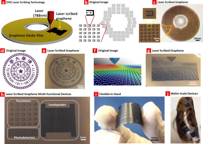
graphene-based electronics, sensors and actuators systems. RESULTS SCALABLE FABRICATION OF LASER SCRIBED GRAPHENE The scalable fabrication of laser scribed graphene is depicted in Figure 1.
The DVD burner containing light scribe function has been used. The 788 nm laser pulses with 5 mW maximum power produced by the burner could convert the stack single-layer GO film into
graphene (Figure 1a). A designed patterning with grayscale, which could control the DVD drive for selective reduction of GO, was import to the software in order to control the patterning
position and laser intensity. As shown in figure 1b, wafer-scale in-plane transistor patterns are designed. After importing the electronic file into the computer software and ~25-minute
laser scribing in DVD burner, graphene transistors are directly patterned on a GO film (Figure 1c). Figure 1d shows the logo of Tsinghua University and the corresponding graphene pattern on
the GO film (Figure 1e). A colored picture and the corresponding laser scribed graphene patterning gray scale are given in Figures 1f and 1g. Figure 1h and 1i show an array of graphene
transistors, an array of photodetectors and a graphene loudspeaker device integrated on a flexible substrate by the direct laser scribing method. The wafer-scale fabrication flexible
graphene-based devices after peeling off with the PET substrate from the DVD disc is shown in Figure 1j. MORPHOLOGY AND STRUCTURE OF LASER SCRIBED GRAPHENE To investigate the morphology and
structure change of the GO film before and after laser scribing, the characterization were performed with SEM, Raman and XPS. The morphology and structure of the laser scribed graphene and
the GO film is illustrated in Figure 2. Figure 2a is the SEM image of laser scribed graphene surface under low magnification. The laser scanning direction is also shown and the patterning
resolution is ~20 μm. Porous structure could be identified in the SEM image of laser scribed graphene surface under high magnification (Figure 2b). And this could be mainly attributed to the
Joule heating that induces the local film expanding by gasification of oxygen species. The surface profile of GO film before laser scribed is shown in Figure 2c, which indicates that the
film is quite uniform with small roughness. As shown in Figure 2d, an increase in laser scribed graphene film thickness is clearly visible in the cross-sectional view of GO and laser scribed
graphene film. The thickness of laser scribed graphene, which is 10 times of the GO film, indicates that a significantly volume expansion related to the gasification of oxygen species
possibly could happen in thickness direction of the GO film during the laser irradiation. The loosely stacked graphene layers could be clearly identified in Figure 2e, the cross-sectional
view of rGO film under high magnification. As can be seen from the cross-sectional view of GO film under high magnification (Figure 2f), the GO film is quite dense, which is quite different
from the loosely stacked graphene layers. Differently, for conventional method to reduce the GO, the temperature applied on GO is increased slowly. The oxygen could release slowly from
reduced graphene oxide to form dense film. Therefore, the thickness of the dense reduce graphene oxide will decrease smoothly due to the loss of oxygen functional group9. In this work, the
laser could give a thermal pulse to GO to increase its temperature in a short time, which is quite different from conventional method. The increase in thickness could be explained by the
rapid generation and release oxygen gases during laser irradiation. When short-time laser treats on small area of GO, the temperature of GO could increase in a short time. As a result, gases
rapidly pass through the film, which could effectively cause the reduced graphene oxide expanding in thickness direction. This process is similar to thermal shock. As shown in figure 2e,
the distance between graphene layers are hundreds of nm, which is loose. There is enough path ways for gas passing away. The Raman spectra of the GO (black line) and laser scribed graphene
(red line) is shown in Figure 2g. GO exhibiting typical D, G and amorphous 2D bands. It is noticed that there is no obvious D band change after the laser scribing. The GO is the carbon
lattice with defect contain oxygen functional groups. The oxygen functional groups break the C-C bond to form obvious D band. After the laser scribing, the C-oxygen functional groups bond
break and oxygen is released. Since there is 10 times thickness expand after laser scribing and laser scribed graphene is loose stack films, C-C recombination is difficult. Hense, there is
no obvious change in D band. It is also noticed that the G band shift to smaller wavenumber, which is due to the reduction of oxygen functional group. The presence of the 2D band indicates
the generation of few-layer graphene. Figure 2h is the TEM image of single-layer laser scribed graphene deposited on carbon TEM grids. The inset of electron diffraction on the graphene film
reveals a hexagonal pattern, which indicates the crystallinity of the graphene. Figure 2i is the TEM image of few-layer GO film deposited on carbon TEM grids. The inset of electron
diffraction on the GO film shows blurred rings. The XPS results of laser scribed graphene and GO are shown in Supplementary Information as Figure S1. Compared with graphene oxide, it is
noticed that oxygen functional group is reduced while C-C sp2 and π-π* bonding are increased significantly in laser scribed graphene17. The laser scribed graphene micro-ribbon with a minimum
patterning resolution of 20 μm is shown in Supplementary Information as Figure S2. The sheet resistance of the graphene micro-ribbon is about 165 Ω per square, which is indicated in the
two-probe electrical measurement of the laser scribed graphene micro-ribbon (20 μm width) in Supplementary Information as Figure S3. TUNABLE RESISTANCE OF LASER SCRIBED GRAPHENE Two-probe
electrical testing are performed on the GO for the sake of demonstrating the electrical resistance tunable ability. And three laser scribed graphene samples which are scribed different times
respectively. The electrical experimental results of the GO film and laser scribed graphene with one, two and three scribing times are shown in Figure 3. The I-V cure of GO film (Figure 3a)
indicates its resistance is 580 MΩ, which means the film could be considered as an insulator. With reference to the I-V cure of laser scribed graphene after one-time patterning (Figure 3b),
the resistance significantly reduces to 8.2 kΩ, which is almost five orders of magnitude decrease compared with GO. Similarly, the resistance of the laser scribed graphene after two-times
patterning reduces to 4.8 kΩ, which is indicated by the I-V cure in Figure 3c. The resistance of laser scribed graphene after three-times patterning reduces to 2.3 kΩ, which is indicated by
the I-V cure in Figure 3d. DIRECT FABRICATION OF IN-PLANE ALL-GRAPHENE TRANSISTORS Previously, most of graphene-based transistors are either back-gate or top gate18,19,20. Since the
back-gate controlling the whole devices, the back-gate transistors have problem of lacking the single transistor control ability. Top-gate graphene-based transistors could be fabricated with
high-k dielectric deposition and metal gate patterning with complex process. Here, we demonstrated a one-step fabrication process of laser scribed in-plane graphene transistors. This kind
of graphene-based in-plane transistor has the advantages of simple process and single transistor control ability. In this in-plane transistor, the laser scribed graphene functions as source,
drain, channel and gate-metal and the GO functions as gate dielectric. The schematic diagrams and experimental results for a laser scribed in-plane graphene transistor are sketched in
Figure 4. The fabrication process for a laser scribed in-plane graphene transistor is depicted in the schematic diagram in Figure 4a. The transfer characteristic for the in-plane graphene
transistor with 0.1 V applied bias voltage Vds is indicated in Figure 4b. As seen in the graph, the Ion/Ioff is up to 5.34, which is much higher than that of most CVD graphene
transistors13,14,15,21 and similar to performance of exfoliated graphene22,23. The transfer curve shows the holes transport with 9.87 cm2V−1s−1 mobility (See detail calculations of the
mobility in Supplementary Information). As the structure defects exist in laser scribed graphene, the low mobility could be reasonable and is similar to the reported results24. It should be
noted that the Dirac point shifts larger than 40 V, which could be explained by the present of residual oxygens those dope the graphene into highly p-type. The frequency dependence of the
specific capacitance of the capacitor in graphene/GO in-plane graphene configuration is shown in Figure S4. As can be seen, the capacitance at 1 kHz frequency is 6.34 × 10⁻⁴ Fm−2. The
Ids–Vds curve recorded for different values of Vig is shown in Figure 4c. Positive gate voltage could lead to lower current and negative gate voltage makes the current higher, which is
consistant with the transfer curve shown in fig. 4b. DIRECT FABRICATION OF GRAPHENE-BASED PHOTODETECTOR Photo-response in graphene has been extensively investigated25,26,27,28,29,30 due to
graphene's wide-band light absorption ability. F. Xia et al. made ultrafast graphene-based photodector by applying laser on graphene field effect transistor31. Nevertheless, the photo
responsivity of the previous graphene photodetectors is too low (typically 0.004 A/W)32. Konstantatos et al. demonstrated 107 A/W photodector by using graphene and quantum dot hydrid system.
Quantum-dot layer absorbs the light, creates electric charges and then transfers to the graphene. The graphene was used as charge transfer layer. Despite all that, how to enhance the pure
graphene photo current is still a critical problem. In this work, stack graphene layer is used to enhance the light absorption. We directly fabricated photodetector using laser scribed
graphene with photo responsivity as high as 0.32 A/W, which is almost two order of magnitude enhancement over the pure graphene result. The schematic diagrams and experimental results for a
laser scribed graphene photodetector is illustrated in Figure 5. Figure 5a is a schematic diagram showing the fabrication process for a laser scribed graphene photodetector. The I-V curves
under laser on and off is shown in Figure 5b, which demonstrated that the positive photocurrent generated when apply laser compared with laser off line. The inset shows the experimental
setup for testing the photodetector. As can be seen in the current versus time under dark and laser cycling in Figure 5c, the photocurrent increases and becomes saturate in a short time when
applying light. And the photocurrent decreases to the initial level when the laser is off. The photo current mapping by changing laser intensity shown in Figure 5d indicates that higher
laser intensity could induce larger photocurrent. The line in the plot of the photo intensity versus the photocurrent (Figure 5e) indicates that the photocurrent increases linearly with the
increasing of the laser intensity. The current response to turning on/off shows exponential rise/fall behaviors (See Supporting information Figure S5, S6). The turning on and off time are
1.45 s and 2.79 s respectively. The photovoltaic effect could be the main mechanism of photocurrent generation in our case (See Supporting information Figure S7, S8). As the laser scribed
graphene could be done in large-scale with precious dimensions, 1-dimensional and 2-dimensional array of photodetectors could be achieved by this method. The schematic structure of a
1-dimensional array of the photodetectors with a light source applied at one end of the array is illustrated in Figure 5f. The inset shows the real optical image of the 23 pixels array. The
length and width of each device are 250 μm and 3000 μm, respectively. The center to center spacing of the neighboring devices is 500 μm. As the photo current versus the position of the
detector from the light shown in Figure 5g, the photocurrent decreases with the increase of the distance from the light source. The inset shows the 1-dimensional pixilation plot, where each
pixel is represented by a device in the array. The schematic structure of a 2-dimentional array of the photodetectors under a light source at center of the array is depicted in Figure 5h.
The inset shows the real optical image of the 3 × 3 pixels array. The 2-dimensional pixilation plot of the 3 × 3 array is shown in Figure 5i. The asymmetric patterns are due to the
dispersion of the light source. It is noticed that the signal in the center is the strongest and the signal is decreased with increasing of the distance from the center. DIRECT FABRICATION
OF GRAPHENE-BASED LOUDSPEAKERS Previously, all the reported graphene loudspeakers need CVD graphene growth and transfer process16,33,34,35, which is time consuming and of low efficiency. A
scalable fabrication process for graphene loudspeakers by laser scribing technology is proposed here. The schematic diagrams and experimental results for a laser scribed graphene loudspeaker
is shown in Figure 6. The fabrication process and experimental setup for a laser scribed graphene loudspeaker is illustrated in the schematic diagram shown in Figure 6a. 5 V sine signal
sweep from 1 to 50 kHz with 5 V bias is applied to graphene to generate the same frequency sound waves. As we can see in the sound spectrum of the graphene loudspeaker (Figure 6b), for 1 to
20 kHz region, the values of sound pressure level (SPL) increase linear with the frequency. And for 20 to 50 kHz region, the SPLs are quite flat. The inset shows the experimental setup for
testing the loudspeaker. The overall trend in the sound spectrum mapping by sweeping the input power (Figure 6c) indicates that the SPLs increase with the input power. And the overall trend
in the sound spectrum mapping by sweeping the measure distance (Figure 6d) indicates that the SPLs decrease with the measure distance. The line in the plot of the sound pressure versus the
input power at 20 kHz sound frequency (Figure 6e) demonstrates that the output sound pressure increases linearly with the increasing of the input power. The line in the plot of the sound
pressure versus the measure distance at 20 kHz sound frequency (Figure S9) demonstrates that there is an inverse relationship between the output sound pressure and measure distance. The
thermoacoustic effect could be the main mechanism of sound generation in our case (See Supporting information Figure S10). DISCUSSION The novelty of this work is the integrating of
wafer-scale high-performance graphene-based in-plane transistors, photodetectors and loudspeakers with one-step fabrication. The achievements in our work are mainly four parts. Firstly, a
laser scribing technology to fabricate wafer-scale grapheme was developed. This laser scribing technology has the advantages of forming graphene in designed shape at precise locations, low
cost with large scale fabrication ability and simple process. Secondly, laser scribed graphene was used to realize all graphene-based large-scale in-plane transistors with high Ion/Ioff
ratio, this parameter is better than that of most CVD graphene13,14,15 (Ion/Ioff ratio ~1.04 ~ 1.4). Thirdly, the large-scale photodetectors and line pixels imaging with high photo
responsivity were achieved with the laser scribed graphene. As far as we know, this is the first demonstration 1-dimentional and 2-dimentional array of graphene photodetectors for photo
imaging. In addition, the responsivity of photodetectors is 2 orders magnitude, which is much better than that of the reported rGO32. Fourthly, the sound generation in a wide range was
realize with laser scribed graphene, of which the sound generation spectrum (1–50 kHz) is 2.5 times wider than that of reported mono-layer graphene on PDMS (1–20 kHz)16. For graphene
in-plane transistors, the higher on/off ratio is on account of the band gap opening of the laser scribed graphene. However, for CVD graphene, there is no band gap. Since GO has a bad gap
larger than 0.5 eV and GO could be partly reduced by the laser, there is band gap for the laser scribed graphene, which could make higher Ion/Ioff ratio than conventional CVD graphene. The
defect in laser scribed graphene is obvious with strong D peak in Raman spectrum, result in the low mobility. The thermal annealing may enhance the mobility to a more reasonable value. The
laser scribed graphene is highly p-doped. In order to make the Dirac-point shift to zero, the chemical n-type doper such as Al could be utilized. For graphene photodetectors, the enhancement
of photo responsibility could be explained by the increasing the density of trap states due to the defects in laser scribed graphene. This could lead to an increase in carrier injection and
transport, thereby producing a larger photo current. For graphene loudspeaker, the wide-band graphene sound generation is attributed to the thermoacoustic effect. Graphene could emit sound
without mechanical vibration, which is fundamental different from conventional acoustic devices. There is a lot of further work could be achieved. Current resolution of the DVD laser
scribing is 20 μm. Smaller resolution is necessary to grow graphene nanoribbon with higher band gap. Smaller laser spot or even e-beam systems could realize nanoscale resolution. Connection
between the graphene multi-functional devices could be made to realize a graphene system. The compatible of laser scribing technology with other conventional CMOS fabrication process needs
to be intensively investigated to make more complex graphene-Si hybrid systems. CONCLUSION From the discussion above, the wafer-scale direct fabrication of graphene-based transistors,
photodetectors and loudspeakers are achieved with a common LightScribe DVD burner. By controlling the pattering times, the resistance of the graphene could be tuned. Laser scribed in-plane
graphene transistors have been demonstrated to have a large on/off ratio up to 5.34. Photo responsivity and specific detectivity as high as 0.32 A/W and 4.996 × 10¹⁰ cmHz1/2W−1 have been
observed in the laser scribed graphene photodetectors. Sound generation of laser scribed graphene is also well demonstrated ranging from 1 to 50 kHz sound frequency. This work indicates that
laser scribing technology could be a powerful and efficient method to integrate high-performance graphene-based devices. METHODS MATERIAL PREPARATION GO dispersion in water with 2 mg/ml
concentration was purchased from XFNANO Materials Tech CO., Ltd (Nanjing, China). GO solutions were synthesized from the graphite powders using a common Hummers method. About 10 mL GO
solutions were drop-casted on the surface of the laser-scribed DVD disc. Then leave the GO solutions overnight to dry on the DVD disc. After that, the GO coated DVD disc could be patterned
by the light-scribed DVD Drive (HP inc. 557S). With the Nero Start Smart software, the designed structure or photograph could be directly converted onto the GO film by laser reducing the GO
into graphene. To fabricate the flexible devices, firstly cover a PET on DVD disc, then drop-casted GO solution and finally laser scribed graphene-based devices and peel it off from the DVD
disc. CHARACTERIZATIONS The surface morphology is observed by Quanta FEG 450 SEM (FEI Inc.). The Raman spectroscopy is obtained using a laser with wavelength of 514.5 nm (HORIBA Inc.).The
XPS is captured by EscaLab 250XI (Thermo Fisher Scientific Inc.). TESTING FOR IN-PLANE TRANSISTORS The electrical testing was done by a standard probe station (Agilent inc. B1500). TESTING
FOR PHOTO-DETECTORS The laser was irradiated on the boundary of the laser-scribed graphene and Ag electrode. The wavelength of the laser was 532 nm. Photocurrents were measured using a
sourcemeter (Keithley 2400). TESTING FOR LOUDSPEAKERS The acoustic platform for testing laser scribed graphene loudspeakers contained a standard microphone and a dynamic signal analyzer. The
1/4 inch standard microphone (Earthworks M50), which had a very flat frequency response reaching up to 50 kHz and a 31 mV/Pa high sensitivity, was used to measure the sound pressure level
of the loudspeakers. The signal analyzer (Agilent 35670A) was used to generate sine signals to drive loudspeakers, make fast Fourier transform analysis and record the value of sound pressure
level. Our test results were measured in a soundproof box. The box size is 1 × 0.5 × 0.5 m3. In order to avoid the effects of reflections, the box was filled with sound-absorbing sponges.
REFERENCES * Geim, A. K. & Novoselov, K. S. The rise of graphene. Nat. Mater. 6, 183–191 (2007). CAS ADS Google Scholar * Bolotin, K. I. et al. Ultrahigh electron mobility in
suspended graphene. Solid State Communications 146, 351–355 (2008). Article CAS ADS Google Scholar * Lee, C., Wei, X., Kysar, J. W. & Hone, J. Measurement of the elastic properties
and intrinsic strength of monolayer graphene. Science 321, 385–388 (2008). Article CAS ADS Google Scholar * Balandin, A. A. et al. Superior thermal conductivity of single-layer graphene.
Nano Lett. 8, 902–907 (2008). Article CAS ADS Google Scholar * Bae, S. et al. Roll-to-roll production of 30-inch graphene films for transparent electrodes. Nat. Nanotechnol. 5, 574–578
(2010). Article CAS ADS Google Scholar * Meric, I. et al. Current saturation in zero-bandgap, top-gated graphene field-effect transistors. Nat. Nanotechnol. 3, 654–659 (2008). Article
CAS ADS Google Scholar * Wu, X. et al. Epitaxial-graphene/graphene-oxide junction: an essential step towards epitaxial graphene electronics. Physical review letters 101, 026801 (2008).
Article ADS Google Scholar * Eda, G., Fanchini, G. & Chhowalla, M. Large-area ultrathin films of reduced graphene oxide as a transparent and flexible electronic material. Nat.
Nanotechnol. 3, 270–274 (2008). Article CAS Google Scholar * Wei, Z. et al. Nanoscale tunable reduction of graphene oxide for graphene electronics. Science 328, 1373–1376 (2010). Article
CAS ADS Google Scholar * Gao, W. et al. Direct laser writing of micro-supercapacitors on hydrated graphite oxide films. Nat. Nanotechnol. 6, 496–500 (2011). Article CAS ADS Google
Scholar * El-Kady, M. F. & Kaner, R. B. Scalable fabrication of high-power graphene micro-supercapacitors for flexible and on-chip energy storage. Nature communications 4, 1475 (2013).
Article ADS Google Scholar * Tian, H. et al. Scalable fabrication of high-performance and flexible graphene strain sensors. Nanoscale, 10.1039/c3nr04521h (2014). * Reina, A. et al. Large
area, few-layer graphene films on arbitrary substrates by chemical vapor deposition. Nano Lett. 9, 30–35 (2008). Article ADS Google Scholar * Yan, Z. et al. Growth of bilayer graphene on
insulating substrates. ACS nano 5, 8187–8192 (2011). Article CAS Google Scholar * Kwak, J. et al. Near room-temperature synthesis of transfer-free graphene films. Nature communications 3,
645 (2012). Article ADS Google Scholar * Suk, J. W., Kirk, K., Hao, Y., Hall, N. A. & Ruoff, R. S. Thermoacoustic sound generation from monolayer graphene for transparent and
flexible sound sources. Advanced Materials 24, 6342–6347 (2012). Article CAS Google Scholar * Strong, V. et al. Patterning and electronic tuning of laser scribed graphene for flexible
all-carbon devices. ACS nano 6, 1395–1403 (2012). Article CAS Google Scholar * Lin, Y.-M. et al. 100-GHz transistors from wafer-scale epitaxial graphene. Science 327, 662–662 (2010).
Article CAS ADS Google Scholar * Das, A. et al. Monitoring dopants by Raman scattering in an electrochemically top-gated graphene transistor. Nat. Nanotechnol. 3, 210–215 (2008). Article
CAS Google Scholar * Schwierz, F. Graphene transistors. Nat. Nanotechnol. 5, 487–496 (2010). Article CAS ADS Google Scholar * Wang, D. et al. Scalable and Direct Growth of Graphene
Micro Ribbons on Dielectric Substrates. Scientific Reports 3, 1348 (2013). Article Google Scholar * Novoselov, K. et al. Electric field effect in atomically thin carbon films. Science 306,
666–669 (2004). Article CAS ADS Google Scholar * Novoselov, K. et al. Two-dimensional gas of massless Dirac fermions in graphene. Nature 438, 197–200 (2005). Article CAS ADS Google
Scholar * Zhang, K. et al. Direct writing of electronic devices on graphene oxide by catalytic scanning probe lithography. Nature communications 3, 1194 (2012). Article ADS Google Scholar
* Mueller, T., Xia, F. & Avouris, P. Graphene photodetectors for high-speed optical communications. Nature Photonics 4, 297–301 (2010). Article CAS Google Scholar * Furchi, M. et
al. Microcavity-integrated graphene photodetector. Nano letters 12, 2773–2777 (2012). Article CAS ADS Google Scholar * Urich, A., Unterrainer, K. & Mueller, T. Intrinsic response
time of graphene photodetectors. Nano letters 11, 2804–2808 (2011). Article CAS ADS Google Scholar * Bonaccorso, F., Sun, Z., Hasan, T. & Ferrari, A. Graphene photonics and
optoelectronics. Nature Photonics 4, 611–622 (2010). Article CAS ADS Google Scholar * Liu, Y. et al. Plasmon resonance enhanced multicolour photodetection by graphene. Nature
communications 2, 579 (2011). Article ADS Google Scholar * Gabor, N. M. et al. Hot carrier–assisted intrinsic photoresponse in graphene. Science 334, 648–652 (2011). Article CAS ADS
Google Scholar * Xia, F., Mueller, T., Lin, Y.-m., Valdes-Garcia, A. & Avouris, P. Ultrafast graphene photodetector. Nat. Nanotechnol. 4, 839–843 (2009). Article CAS ADS Google
Scholar * Chitara, B., Panchakarla, L., Krupanidhi, S. & Rao, C. Infrared photodetectors based on reduced graphene oxide and graphene nanoribbons. Advanced Materials 23, 5419–5424
(2011). Article CAS Google Scholar * Tian, H. et al. Graphene-on-paper sound source devices. ACS nano 5, 4878–4885 (2011). Article CAS Google Scholar * Tian, H. et al. Single-layer
graphene sound-emitting devices: experiments and modeling. Nanoscale 4, 2272–2277 (2012). Article CAS ADS Google Scholar * Tian, H. et al. Static behavior of a graphene-based
sound-emitting device. Nanoscale 4, 3345–3349 (2012). Article CAS ADS Google Scholar Download references ACKNOWLEDGEMENTS This work was supported by the National Natural Science
Foundation of China (61025021, 60936002, 51072089 and 61020106006), the National Key Project of Science and Technology (2011ZX02403-002) the Special Fund for Agro-scientific Research in the
Public Interest (201303107). He Tian is additionally supported by the Ministry of Education Scholarship of China. Thanks for the valuable discussions with Prof. Z. Bao from Stanford
University. AUTHOR INFORMATION AUTHORS AND AFFILIATIONS * Institute of Microelectronics, Tsinghua University, Beijing, 100084, China He Tian, Yi Yang, Dan Xie, Ya-Long Cui, Wen-Tian Mi &
Tian-Ling Ren * Tsinghua National Laboratory for Information Science and Technology (TNList), Tsinghua University, Beijing, 100084, China He Tian, Yi Yang, Dan Xie, Ya-Long Cui, Wen-Tian Mi
& Tian-Ling Ren * The Molecular Foundry, Lawrence Berkeley National Laboratory, 1 Cyclotron Road, 94720, Berkeley, CA, USA Yuegang Zhang * Suzhou Institute of Nano-Tech and
Nano-Bionics, Chinese Academy of Sciences, Suzhou, 215123, China Yuegang Zhang Authors * He Tian View author publications You can also search for this author inPubMed Google Scholar * Yi
Yang View author publications You can also search for this author inPubMed Google Scholar * Dan Xie View author publications You can also search for this author inPubMed Google Scholar *
Ya-Long Cui View author publications You can also search for this author inPubMed Google Scholar * Wen-Tian Mi View author publications You can also search for this author inPubMed Google
Scholar * Yuegang Zhang View author publications You can also search for this author inPubMed Google Scholar * Tian-Ling Ren View author publications You can also search for this author
inPubMed Google Scholar CONTRIBUTIONS H.T. made and tested the samples, performed simulations and drafted the manuscript. T.-L.R. and Y.Z. oversaw all research phases, optimized the devices
performance and revised the manuscript. D.X., Y.Y., Y.-L.C. and W.-T.M. analyzed the test results and revised the manuscript. All authors discussed and commented on the manuscript. ETHICS
DECLARATIONS COMPETING INTERESTS The authors declare no competing financial interests. ELECTRONIC SUPPLEMENTARY MATERIAL SUPPLEMENTARY INFORMATION Supplementary_Information RIGHTS AND
PERMISSIONS This work is licensed under a Creative Commons Attribution-NonCommercial-NoDerivs 3.0 Unported License. To view a copy of this license, visit
http://creativecommons.org/licenses/by-nc-nd/3.0/ Reprints and permissions ABOUT THIS ARTICLE CITE THIS ARTICLE Tian, H., Yang, Y., Xie, D. _et al._ Wafer-Scale Integration of Graphene-based
Electronic, Optoelectronic and Electroacoustic Devices. _Sci Rep_ 4, 3598 (2014). https://doi.org/10.1038/srep03598 Download citation * Received: 16 October 2013 * Accepted: 09 December
2013 * Published: 08 January 2014 * DOI: https://doi.org/10.1038/srep03598 SHARE THIS ARTICLE Anyone you share the following link with will be able to read this content: Get shareable link
Sorry, a shareable link is not currently available for this article. Copy to clipboard Provided by the Springer Nature SharedIt content-sharing initiative