Spin injection in graphene using ferromagnetic van der waals contacts of indium and cobalt
- Select a language for the TTS:
- UK English Female
- UK English Male
- US English Female
- US English Male
- Australian Female
- Australian Male
- Language selected: (auto detect) - EN
Play all audios:

ABSTRACT Graphene-based spintronic devices require efficient spin injection, and dielectric tunnel barriers are typically used to facilitate spin injection. However, the direct growth of
ultrathin dielectrics on two-dimensional surfaces is challenging and unreliable. Here we report spin injection in graphene lateral spin valves using ferromagnetic van der Waals contacts of
indium and cobalt (In–Co), and without the deposition of dielectric tunnel barriers. With this approach, we obtain magnetoresistance values of 1.5% ± 0.5% (spin signal around 50 Ω), which is
comparable to state-of-the-art graphene lateral spin valves with oxide tunnel barriers, with a working device yield of more than 70%. By contrast, lateral spin valves with non-van der Waals
contacts containing only cobalt are inefficient and exhibit, at best, a magnetoresistance of around 0.2% (spin signal around 3 Ω). The contact resistance of our ferromagnetic indium–cobalt
van der Waals contacts is 2–5 kΩ, which makes them compatible with complementary metal–oxide–semiconductor devices. SIMILAR CONTENT BEING VIEWED BY OTHERS SPIN FILTERING BY PROXIMITY EFFECTS
AT HYBRIDIZED INTERFACES IN SPIN-VALVES WITH 2D GRAPHENE BARRIERS Article Open access 09 November 2020 ALL-ELECTRICAL CREATION AND CONTROL OF SPIN-GALVANIC SIGNAL IN GRAPHENE AND MOLYBDENUM
DITELLURIDE HETEROSTRUCTURES AT ROOM TEMPERATURE Article Open access 08 June 2021 OBLIQUE SPIN INJECTION TO GRAPHENE VIA GEOMETRY CONTROLLED MAGNETIC NANOWIRES Article Open access 25 July
2024 MAIN Creating clean metal contacts to semiconductors is central to modern electronics1. These metal–semiconductor heterojunctions are governed by energy-level alignments across the
contact interface. However, dangling bonds and metallization induced defects lead to chemical reactions, interdiffusion and localized strain, which prevent the interface from being
atomically sharp2,3. These issues are exacerbated for metal contacts on two-dimensional (2D) materials because atomically thin semiconductors are easily damaged during metal deposition2,3.
Van der Waals (vdW) contacts can, however, be used to create ultra-clean interfaces with 2D semiconductors4,5. Such vdW contacts are characterized by the presence of a 2–4 Å vacuum gap
between the metal and 2D semiconductor, and vdW contacts fabricated by mechanical transfer of metals2, by using metallic 2D materials6, and by direct metal deposition of indium alloys4,5
have been shown to decrease contact resistance and improve device performance. Spin-based devices are of potential use in the development of energy-efficient computing7,8,9 and graphene has
been explored for such spintronic devices because of its long spin diffusion lengths9,10,11. For efficient injection of spin-polarized electrons in lateral spin valves (LSVs), the
conductivity mismatch between the ferromagnetic (FM) metal contact and graphene channel must be overcome to avoid spin backflow and interfacial spin flipping12,13. This is typically done by
inserting thin tunnel barriers of magnesium oxide (MgO), titanium dioxide (TiO2) or aluminium oxide (Al2O3) between the metal contact and the spin channel12,14. Graphene is, however, free of
dangling bonds and therefore uniform deposition of ultrathin oxide thin films is challenging15,16. As a result, the yield of working graphene-based LSVs utilizing oxide tunnel barriers is
low (typically less than 10%)9,17,18. In addition, remote interface phonon coupling and charge impurity/defect scattering at the oxide interface adversely affects the transport of
spin-polarized carriers in graphene. Inserting mechanically transferred hexagonal boron nitride (h-BN) between cobalt and graphene has been shown to inject spins19,20,21,22. LSVs have also
been created with one 2D FM Fe5GeTe2 electrode and one Co/TiO2 electrode on graphene23, which suggests that the vdW vacuum gap between 2D Fe5GeTe2 and graphene can act as a tunnel barrier
for efficient spin injection. We have previously shown that indium alloy vdW contacts on 2D materials can have a vacuum gap between the metal and the semiconductor5. Such indium alloy vdW
contacts exhibit low contact resistance and are free from Fermi level pinning. They can also be used to create high-performance p- and n-type field effect transistors (FETs)3,4,5. In this
Article, we show that vdW contacts of FM indium/cobalt (In/Co) can be fabricated by industry-compatible electron beam evaporation on graphene and can be used to inject spins. With our FM
In/Co vdW contacts, we can repeatably obtain magnetoresistance (MR) values of 1.5% ± 0.5%, which is comparable to state-of-the-art graphene lateral spin valves with oxide tunnel
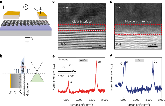
barriers24,25,26. FERROMAGNETIC VDW CONTACTS We fabricated LSVs (Fig. 1a,b) using mechanically exfoliated graphene and FM In/Co electrodes of dissimilar widths (and hence dissimilar
coercivities) as vdW contacts for spin injection and collection (see methods for details of device fabrication). We characterized the cross-sectional interface of the In/Co contacts using
high-resolution annular bright-field (ABF) scanning transmission electron microscopy (STEM). The image in Fig. 1c, which corresponds to the red rectangle in Fig. 1a, shows that In/Co
contacts form a clean vdW interface with graphene. By contrast, the interface between graphene and Co (Fig. 1d) is disordered. Multiple locations of the cross-sectional interface were
characterized using STEM to confirm the uniformity of In/Co metal films on graphene (shown in Supplementary Fig. 1). The energy-dispersive X-ray spectroscopy (EDS) mapping of the interface
shown in Supplementary Fig. 2 indicates that the In and Co are homogeneously mixed. Raman spectroscopy is widely used to characterize the structural quality and doping levels of graphene27.
The Raman spectrum (Fig. 1e) of graphene measured through In/Co exhibits a single Lorentzian 2D peak at 2,671 cm−1 and the intensity ratio of the 2D peak to the G peak, _I_2D/_I_G is 2.5,
which suggests a doping level of ~150 meV and carrier concentration of ~1012 cm−2 (curve fitting is described in Supplementary Fig. 3). This is similar to the Raman spectrum of pristine
graphene on SiO2 (_I_2D/_I_G is 2.8) shown in the inset. The damage and disorder at the Co/graphene interface is confirmed by Raman via splitting of the G band and the appearance of the G′
mode (Fig. 1f) (Supplementary Section 3). Furthermore, the position of the 2D mode softens to 2,660 cm−1 and _I_2D/_I_G decreases to 1.0 after Co deposition on graphene. An _I_2D/_I_G of 1.0
corresponds to about 700 meV shift in the Fermi energy, which increases the carrier concentration to ~1013 cm−2. The large carrier density decreases the contact resistance and therefore
reduces the barrier for spin injection28. In contrast, In/Co forms a vdW contact with graphene with a vacuum gap of ~0.3 nm (see Supplementary Section 4 for a schematic of the interface).
ELECTRICAL TRANSPORT ACROSS FERROMAGNETIC VDW CONTACTS The optical micrograph of a typical LSV device is shown in Fig. 2a, where six In/Co contacts of dissimilar widths were deposited on
graphene. In/Au contacts were also included for control experiments. Graphene flakes used in this study are hole doped with a room-temperature field effect mobility of 2,000 ± 500 cm2 Vs−1
as indicated by the backgated FET transfer characteristics shown in Fig. 2b (refs. 29,30). The resistance at zero gate bias was found to be 2 kΩ, which is lower than graphene LSV devices
with tunnel barrier contacts, in which resistances typically range from tens of kΩ to a few hundreds of MΩ (refs. 25,31). Next, to understand the nature of carrier transport with In/Co vdW
contacts, we performed temperature-dependent measurements. Current–voltage (_I_–_V_) measurements from 10 K to 300 K are shown in Fig. 2c. Weak temperature dependence and a non-ohmic
behaviour at low bias are observed. The temperature dependence is shown in the inset, where the resistance enhancement (_R_/_R_300K) measured at a bias of 10 mV is <1.4 and is almost
constant below 100 K. The weak temperature dependence is further corroborated by the plot of current versus 1,000/_T_ in Supplementary Fig. 5a. The non-ohmic transport is also evident in the
voltage dependence of differential conductance (d_I_/d_V_) at 10 K shown in Fig. 2d, where the decrease in conductance at low bias is a signature of tunnelling transport15,32. By contrast,
the voltage dependence of d_I_/d_V_ for pure cobalt contacts is relatively flat, suggesting absence of a potential barrier at the interface. The voltage dependence of conductance was fit
with the Brinkman, Dynes and Rowell model33 for an asymmetric barrier, as shown in Supplementary Section 6, from which an effective barrier height, _φ_, of ~50 meV was extracted. The device
conductance also shows very weak temperature dependence (Supplementary Fig. 5b,c), suggesting tunnelling at the FM vdW contact interface22. These electrical transport properties suggest
field-assisted tunnelling as the dominant electron transport mechanism with FM In/Co vdW contacts34. SPIN TRANSPORT IN GRAPHENE LSVS Magneto-optical Kerr effect (MOKE) magnetometry was used
to investigate the magnetic switching of In/Co electrodes at room temperature. The magnetic field was applied parallel to the in-plane easy axis of the FM contacts (along the _y_ axis in
Fig. 2a). The hysteresis loops (Fig. 3a and Supplementary Fig. 7) suggest uniaxial anisotropy with both contacts switching magnetization at magnetic fields of 10–20 mT. The wider electrodes
show lower coercive fields (grey curve) compared to the narrow electrodes (black curve) due to shape anisotropy. From this, the magnetic field required to pin the FM contacts in parallel and
antiparallel spin orientations can be estimated. Spin transport across a non-magnetic semiconductor can be probed by measuring the change in resistance induced by change in orientation of
the magnetic field (parallel to antiparallel configuration)11. MR characteristics of graphene LSVs were obtained by measuring the resistance of the graphene spin channel while sweeping the
magnetic field in-plane (along the _y_ direction parallel to the magnetic easy axis, as shown in Fig. 2a) at 4 K. The magnetic field dependence of resistance for devices with Co only and
In/Co contacts is shown in Fig. 3b. As the magnetic field is decreased and increased (red and black curves), we observe two clear transitions in the device resistance. The resistance versus
magnetic field characteristics shown in the upper panel of Fig. 3b from one of the few working devices with cobalt-only contacts show an MR of 0.1% (spin signal of 3 Ω). In comparison, an MR
of 2% (spin signal of 50 Ω) is found in In/Co-contacted devices, as shown in the lower panel of Fig. 3b. The channel lengths for our LSVs are 2 μm, and the MR obtained is comparable to a
device with a 2-μm-long spin channel made of epitaxial graphene with Co/Al2O3 tunnel barrier contacts25. Our In/Co device results are remarkable because no tunnel barrier is used, and they
demonstrate that the vdW vacuum gap is sufficient for efficient spin injection. The measured MR is attributed to the spin valve effect, where the resistance of the spin-polarized electrons
in the channel changes according to the relative spin orientation of the FM contacts and exhibits a transition during magnetization switching. The fields at which these transitions occur
correspond to the coercive fields for 180° magnetization switching of the FM vdW contacts measured by MOKE (Fig. 3a), suggesting that the MR observed is due to spin transport. The gate
dependence of magneto transport (Supplementary Section 8) shows an increase in spin signal near the Dirac peak region, which provides additional evidence of tunnelling transport across the
In/Co and graphene interface26. We have also performed four terminal, non-local spin diffusion measurements, which show MR peaks that switch at magnetic fields identical to local LSVs
(Supplementary Fig. 10). We have measured the non-local spin signal from In/Co-based graphene LSVs at 10 K as a function of injection current from 1 μA to 25 μA (Supplementary Fig. 11). The
linear bias dependence of the non-local signal indicates that our spin signals are not related to thermal effects35. Further, we have performed MR measurements for LSVs with FM In/Co contact
at one end and a non-magnetic In/Au contact at another end. These devices do not show any spin signals (Supplementary Fig. 12). All of the above results indicate that the MR observed in our
graphene LSVs with In/Co contacts originates from spin-polarized transport in graphene32. Notably, the MR in our devices shows a decrease in resistance for antiparallel spin orientations of
the contacts (Fig. 3b). Although this contradicts the standard Julliere model36, negative MR peaks in graphene LSV devices are not uncommon32,36. Negative MR can be attributed to quantum
interference in the spin channel, where the sign of the MR could be related to the sign of the spin polarization at the interface between contacts and graphene37,38,39. We have measured four
terminal non-local Hanle spin precession signals for the In/Co-based graphene LSVs at 10 K, as shown in Supplementary Fig. 13, which were fitted with the Hanle spin transport equation10
(Supplementary Section 12) to obtain the spin lifetime and spin diffusion lengths. The spin lifetime and spin diffusion lengths for In/Co-based LSVs were found to be ~200 ps and 2.4 μm,
respectively, which are similar to the values reported in the literature15,22. We have observed MR at room temperature, as shown in the temperature-dependent measurements of the non-local
spin signal provided in Supplementary Section 13. While the spin signal and switching field are lower than at 4 K due to spin scattering, lower barrier height and temperature-dependent
increase of coercivity (Supplementary Fig. 15), our results show that spin injection and transport at room temperature is possible with vdW In/Co contacts. The magnitude of the MR in our
LSVs is dependent on the applied bias, as shown in Fig. 4a. As the current sourced is increased from 10 nA to 10 μA, we see consistent spin valve signals at similar switching fields, but the
MR reduces at higher current biases. Sourcing higher currents leads to an increase in the applied potential bias across the interface barrier. At higher bias, we observe a rapid decrease of
the spin signal from 20 Ω to 8 Ω, while the resistance of the parallel spin state reduces only slightly from 2.34 kΩ to 2.27 kΩ (shown in Fig. 4b). Similar bias dependence has been observed
in magnetic tunnel junctions and LSVs with tunnel contacts32,40,41,42. To highlight the ease of using vdW contacts for spin injection, the MR values at different biases for 15 In/Co devices
are summarized in Fig. 4c. The MR from four Co-contacted devices are also shown for comparison. For the In/Co vdW contact-based LSVs a rapid increase of MR at low bias up to 2% is observed
and all our devices exhibit similar bias dependence with negligible variation. On the contrary, the MR from cobalt-based devices is lower, ≤0.2%, even at low biases (orange shaded region).
Typically, we fabricate ten devices per batch. In most batches, >70% of devices show clear spin valve signals (see Supplementary Table 1 for device statistics from 23 devices). The
switching fields for all our devices are similar in the range of 20–30 mT. By contrast, the yield of working devices with contacts containing only Co is substantially lower, at <10%. The
statistical distribution of MR and two terminal resistances for graphene LSVs with In/Co contacts is shown in Fig. 4d, in the form of histograms. The distribution peaks at 1.2% for MR and
2.8 kΩ for contact resistance. The low contact resistance can be attributed to the low effective barrier height resulting from the vacuum vdW gap for In/Co contacts. Such contact resistance
is orders of magnitude lower than oxide or h-BN tunnel barrier contacts needed to achieve a similar MR. A comparison of MR and resistance area (RA) product of In/Co vdW contacts (shown in
Fig. 4e) with previously reported spin-injection contacts based on oxide dielectrics or 2D tunnel barriers, such as h-BN, reveals that In/Co contacts possess good MR and low contact
resistance. CONCLUSIONS We have reported a scalable technique to deposit FM In/Co vdW contacts on graphene. The vdW contact enables robust and reproducible spin injection in graphene LSVs
without the need for an additional tunnel barrier. The contact resistance in our devices is lower than in conventional LSVs. This is noteworthy because ultrahigh resistance tunnel contact
devices are incompatible with complementary metal–oxide–semiconductor devices. Spintronic devices with vdW In/Co FM contacts could provide better impedance matching with
low-contact-resistance FETs, faster device operation and improved spin current–energy conversion efficiency43, and our work highlights the potential of using a van der Waals gap as a
tunnelling medium in spintronic devices. METHODS SAMPLE PREPARATION AND DEVICE FABRICATION Monolayer graphene flakes were mechanically exfoliated from a high-quality bulk graphite crystal
using M/H Ultron tape. The substrates were lithographically prepatterned 90/300 nm SiO2 on heavily doped Si, which were used as gate insulator and electrode, respectively. Monolayer graphene
flakes were identified using optical microscopy, atomic force microscopy and Raman spectroscopy. The samples were coated with MMA/PMMA resist and electron beam lithography was used to
pattern the electrodes. Before metal electrode deposition, the electron beam evaporation system was pumped to a base pressure of <10−7 Torr. Then, 8–10-nm-thick In was deposited with a
low rate of 0.1 Å s−1 and 40-nm-thick Co was deposited subsequently. Finally, 5-nm-thick Au was deposited to prevent oxidation of cobalt. The device was rinsed with isopropanol after
immersing in acetone for lift-off. RAMAN SPECTROSCOPY Raman spectra were acquired using a Renishaw inVIA microRaman spectrometer. The samples were excited with a 514 nm laser with the power
kept below 100 μW. A 2,400 lines per mm grating was used to record the spectra. For collecting the spectra from metal-coated graphene, thin layers (10–15 nm) of metals (Co, In/Co and In/Au)
were deposited to ensure optical transparency. TRANSPORT MEASUREMENTS Electrical transport characteristics were measured using a Keithley 4200 semiconductor parameter analyser system in an
ambient probe station. The low-temperature measurements were performed in a Lakeshore cryogenic vacuum probe station with a closed cycle compressor and a Lakeshore temperature controller.
Magneto transport measurements were performed using a Quantum Design Dynacool PPMS. MAGNETO-OPTIC KERR EFFECT MICROSCOPY Magnetic hysteresis loops were obtained from measurements of the
longitudinal magneto-optic Kerr effect using a nanoMOKE 2 magnetometer, produced by Durham Magneto Optics. The laser spot was focused to a full-width at half-maximum diameter of ~5 μm and
individual electrodes were located optically. The magnetic field was applied in-plane and along the long axes of the FM electrodes, parallel to their magnetic easy axis. MOKE data shown in
this work are the result of taking the average of 50 individual hysteresis loops in quick succession. STEM SAMPLE PREPARATION AND ACQUISITION PARAMETERS The cross-sectional TEM specimens
were fabricated using a focused ion beam (Hitachi Triple Beam NX2000). The condition of the Ga ion beam used in the last fine milling process was 3 kV, 40 pA. The damage to the sample was
minimized under the conditions of low voltage and current. STEM images and EDS mapping images were taken by a FEI Titan3 G2 60–300 at an accelerating voltage of 200 kV. ABF-STEM images were
acquired with an acceptance semi-angle of the detector range from 10 to 61 mrad. DATA AVAILABILITY The data that support the plots within this paper and other findings of the study are
available from the corresponding authors upon reasonable request. CODE AVAILABILITY The codes used for plotting the data are available from the corresponding authors upon reasonable request.
REFERENCES * Sze, S. M., Li, Y. & Ng, K. K. _Physics of Semiconductor Devices_ (Wiley, 2021). * Liu, Y. et al. Approaching the Schottky–Mott limit in van der Waals metal–semiconductor
junctions. _Nature_ 557, 696–700 (2018). Article MATH Google Scholar * Wang, Y. & Chhowalla, M. Making clean electrical contacts on 2D transition metal dichalcogenides. _Nat. Rev.
Phys._ 4, 101–112 (2022). Article Google Scholar * Wang, Y. et al. P-type electrical contacts for 2D transition-metal dichalcogenides. _Nature_ 610, 61–66 (2022). Article MATH Google
Scholar * Wang, Y. et al. Van der Waals contacts between three-dimensional metals and two-dimensional semiconductors. _Nature_ 568, 70–74 (2019). Article MATH Google Scholar * Cui, X. et
al. Multi-terminal transport measurements of MoS2 using a van der Waals heterostructure device platform. _Nat. Nanotechnol._ 10, 534–540 (2015). Article MATH Google Scholar * Sahoo, S.
et al. Electric field control of spin transport. _Nat. Phys._ 1, 99–102 (2005). Article MATH Google Scholar * Alphenaar, B. W. et al. Magnetoresistance of ferromagnetically contacted
carbon nanotubes. _Phys. E_ 10, 499–504 (2001). Article Google Scholar * Hill, E. et al. Graphene spin valve devices. _IEEE Trans. Magn._ 42, 2694–2696 (2006). Article MATH Google
Scholar * Avsar, A. et al. Colloquium: spintronics in graphene and other two-dimensional materials. _Rev. Mod. Phys._ 92, 021003 (2020). Article MATH Google Scholar * Han, W., Kawakami,
R. K., Gmitra, M. & Fabian, J. Graphene spintronics. _Nat. Nanotechnol._ 9, 794–807 (2014). Article Google Scholar * Rashba, E. I. Theory of electrical spin injection: tunnel contacts
as a solution of the conductivity mismatch problem. _Phys. Rev. B_ 62, R16267–R16270 (2000). Article MATH Google Scholar * Schmidt, G., Ferrand, D., Molenkamp, L., Filip, A. & Van
Wees, B. Fundamental obstacle for electrical spin injection from a ferromagnetic metal into a diffusive semiconductor. _Phys. Rev. B_ 62, R4790 (2000). Article Google Scholar * Fert, A.
& Jaffres, H. Conditions for efficient spin injection from a ferromagnetic metal into a semiconductor. _Phys. Rev. B_ 64, 184420 (2001). Article Google Scholar * Friedman, A. L., van’t
Erve, O. M., Li, C. H., Robinson, J. T. & Jonker, B. T. Homoepitaxial tunnel barriers with functionalized graphene-on-graphene for charge and spin transport. _Nat. Commun._ 5, 3161
(2014). Article Google Scholar * Li, W. et al. Uniform and ultrathin high-κ gate dielectrics for two-dimensional electronic devices. _Nat. Electron._ 2, 563–571 (2019). Article MATH
Google Scholar * Ahn, E. C. 2D materials for spintronic devices. _npj 2D Mater. Appl._ 4, 17 (2020). Article MATH Google Scholar * Gurram, M., Omar, S. & van Wees, B. J. Electrical
spin injection, transport, and detection in graphene-hexagonal boron nitride van der Waals heterostructures: progress and perspectives. _2D Mater._ 5, 032004 (2018). Article Google Scholar
* Kamalakar, M. V., Dankert, A., Bergsten, J., Ive, T. & Dash, S. P. Spintronics with graphene-hexagonal boron nitride van der Waals heterostructures. _Appl. Phys. Lett._ 105, 212405
(2014). Article Google Scholar * Singh, S. et al. Nanosecond spin relaxation times in single layer graphene spin valves with hexagonal boron nitride tunnel barriers. _Appl. Phys. Lett._
109, 122411 (2016). Article Google Scholar * Fu, W., Makk, P., Maurand, R., Bräuninger, M. & Schönenberger, C. Large-scale fabrication of BN tunnel barriers for graphene spintronics.
_J. Appl. Phys._ 116, 074306 (2014). Article Google Scholar * Kamalakar, M. V., Dankert, A., Bergsten, J., Ive, T. & Dash, S. P. Enhanced tunnel spin injection into graphene using
chemical vapor deposited hexagonal boron nitride. _Sci. Rep._ 4, 6146 (2014). Article Google Scholar * Zhao, B. et al. Temperature spin‐valve with van der Waals ferromagnet
Fe5GeTe2/graphene heterostructure. _Adv. Mater._ 35, 2209113 (2023). Article Google Scholar * Tombros, N., Jozsa, C., Popinciuc, M., Jonkman, H. T. & Van Wees, B. J. Electronic spin
transport and spin precession in single graphene layers at room temperature. _Nature_ 448, 571–574 (2007). Article Google Scholar * Dlubak, B. et al. Highly efficient spin transport in
epitaxial graphene on SiC. _Nat. Phys._ 8, 557–561 (2012). Article MATH Google Scholar * Han, W. et al. Tunneling spin injection into single layer graphene. _Phys. Rev. Lett._ 105, 167202
(2010). Article Google Scholar * Das, A. et al. Monitoring dopants by Raman scattering in an electrochemically top-gated graphene transistor. _Nat. Nanotechnol._ 3, 210–215 (2008).
Article MATH Google Scholar * Shen, P. et al. Ultralow contact resistance between semimetal and monolayer semiconductors. _Nature_ 593, 211–217 (2021). Article MATH Google Scholar *
Yang, Y., Brenner, K. & Murali, R. The influence of atmosphere on electrical transport in graphene. _Carbon_ 50, 1727–1733 (2012). Article MATH Google Scholar * Han, W. et al. Spin
transport and relaxation in graphene. _J. Magn. Magn. Mater._ 324, 369–381 (2012). Article MATH Google Scholar * Yan, W. et al. Long spin diffusion length in few-layer graphene flakes.
_Phys. Rev. Lett._ 117, 147201 (2016). Article Google Scholar * Wang, W. et al. Magnetotransport properties of mesoscopic graphite spin valves. _Phys. Rev. B_ 77, 020402 (2008). Article
MATH Google Scholar * Brinkman, W., Dynes, R. & Rowell, J. Tunneling conductance of asymmetrical barriers. _J. Appl. Phys._ 41, 1915–1921 (1970). Article MATH Google Scholar * Omar,
S. & van Wees, B. J. Graphene-WS2 heterostructures for tunable spin injection and spin transport. _Phys. Rev. B_ 95, 081404 (2017). Article MATH Google Scholar * Slachter, A.,
Bakker, F. L., Adam, J.-P. & van Wees, B. J. Thermally driven spin injection from a ferromagnet into a non-magnetic metal. _Nat. Phys._ 6, 879–882 (2010). Article Google Scholar *
Julliere, M. Tunneling between ferromagnetic films. _Phys. Lett. A_ 54, 225–226 (1975). Article MATH Google Scholar * De Teresa, J. M. et al. Role of metal-oxide interface in determining
the spin polarization of magnetic tunnel junctions. _Science_ 286, 507–509 (1999). Article MATH Google Scholar * Xu, J. et al. Spin inversion in graphene spin valves by gate-tunable
magnetic proximity effect at one-dimensional contacts. _Nat. Commun._ 9, 2869 (2018). Article MATH Google Scholar * Schäpers, T., Nitta, J., Heersche, H. & Takayanagi, H. Interference
ferromagnet/semiconductor/ferromagnet spin field-effect transistor. _Phys. Rev. B_ 64, 125314 (2001). Article MATH Google Scholar * Zhang, S., Levy, P., Marley, A. & Parkin, S.
Quenching of magnetoresistance by hot electrons in magnetic tunnel junctions. _Phys. Rev. Lett._ 79, 3744 (1997). Article MATH Google Scholar * Moodera, J. S., Kinder, L. R., Wong, T. M.
& Meservey, R. Large magnetoresistance at room temperature in ferromagnetic thin film tunnel junctions. _Phys. Rev. Lett._ 74, 3273 (1995). Article Google Scholar * Lu, Y. et al. Bias
voltage and temperature dependence of magnetotunneling effect. _J. Appl. Phys._ 83, 6515–6517 (1998). Article MATH Google Scholar * Komatsu, K. et al. Spin injection and detection in a
graphene lateral spin valve using an yttrium-oxide tunneling barrier. _Appl. Phys. Express_ 7, 085101 (2014). Article MATH Google Scholar * Singh, S. et al. Strontium oxide tunnel
barriers for high quality spin transport and large spin accumulation in graphene. _Nano Lett._ 17, 7578–7585 (2017). Article MATH Google Scholar Download references ACKNOWLEDGEMENTS M.C.
acknowledges funding from European Research Council (ERC) Advanced Grant under the European Union’s Horizon 2020 research and innovation programme (grant agreement GA 101019828-2D- LOTTO),
EPSRC (EP/ T026200/1, EP/T001038/1) and grant supported by the Department of Science, Innovation and Technology and the Royal Academy of Engineering under the Chair in Emerging Technologies
programme. H.Y.J. acknowledges support from the National R&D Program through the National Research Foundation of Korea funded by the Ministry of Science and ICT (2022M3H4A1A01013228). We
thank N. D. Mathur and R. Mishra for discussions about the results. AUTHOR INFORMATION AUTHORS AND AFFILIATIONS * Department of Materials Science & Metallurgy, University of Cambridge,
Cambridge, UK Soumya Sarkar, Yang Li, Yiru Zhu, Maheera Abdul Ghani, Han Yan, Yan Wang & Manish Chhowalla * Graduate School of Semiconductor Materials and Devices Engineering, Ulsan
National Institute of Science and Technology (UNIST), Ulsan, Republic of Korea Saeyoung Oh & Hu Young Jeong * Department of Physics, Cavendish Laboratory, University of Cambridge,
Cambridge, UK Peter J. Newton Authors * Soumya Sarkar View author publications You can also search for this author inPubMed Google Scholar * Saeyoung Oh View author publications You can also
search for this author inPubMed Google Scholar * Peter J. Newton View author publications You can also search for this author inPubMed Google Scholar * Yang Li View author publications You
can also search for this author inPubMed Google Scholar * Yiru Zhu View author publications You can also search for this author inPubMed Google Scholar * Maheera Abdul Ghani View author
publications You can also search for this author inPubMed Google Scholar * Han Yan View author publications You can also search for this author inPubMed Google Scholar * Hu Young Jeong View
author publications You can also search for this author inPubMed Google Scholar * Yan Wang View author publications You can also search for this author inPubMed Google Scholar * Manish
Chhowalla View author publications You can also search for this author inPubMed Google Scholar CONTRIBUTIONS M.C. proposed the research and supervised the project. S.S. prepared and
characterized samples, fabricated, measured devices and interpreted results. Y.W. assisted in device fabrication and interpreted results. S.O. prepared samples using focused ion beam and
performed cross-sectional STEM with guidance from H.Y.J. P.J.N. performed MOKE measurements. Y.L., M.A.G. and Y.Z. assisted in measurements. H.Y. prepared the lithographically prepatterned
substrates. S.S. and M.C. wrote the paper. All authors read the paper and agreed on its content. CORRESPONDING AUTHORS Correspondence to Soumya Sarkar, Yan Wang or Manish Chhowalla. ETHICS
DECLARATIONS COMPETING INTERESTS The authors declare no competing interests. PEER REVIEW PEER REVIEW INFORMATION _Nature Electronics_ thanks Ahmet Avsar, Biplab Sanyal and the other,
anonymous, reviewer(s) for their contribution to the peer review of this work. ADDITIONAL INFORMATION PUBLISHER’S NOTE Springer Nature remains neutral with regard to jurisdictional claims in
published maps and institutional affiliations. SUPPLEMENTARY INFORMATION SUPPLEMENTARY INFORMATION Supplementary Figs. 1–15 and Table 1. RIGHTS AND PERMISSIONS OPEN ACCESS This article is
licensed under a Creative Commons Attribution 4.0 International License, which permits use, sharing, adaptation, distribution and reproduction in any medium or format, as long as you give
appropriate credit to the original author(s) and the source, provide a link to the Creative Commons licence, and indicate if changes were made. The images or other third party material in
this article are included in the article’s Creative Commons licence, unless indicated otherwise in a credit line to the material. If material is not included in the article’s Creative
Commons licence and your intended use is not permitted by statutory regulation or exceeds the permitted use, you will need to obtain permission directly from the copyright holder. To view a
copy of this licence, visit http://creativecommons.org/licenses/by/4.0/. Reprints and permissions ABOUT THIS ARTICLE CITE THIS ARTICLE Sarkar, S., Oh, S., Newton, P.J. _et al._ Spin
injection in graphene using ferromagnetic van der Waals contacts of indium and cobalt. _Nat Electron_ 8, 215–221 (2025). https://doi.org/10.1038/s41928-024-01330-w Download citation *
Received: 06 July 2023 * Accepted: 03 December 2024 * Published: 20 January 2025 * Issue Date: March 2025 * DOI: https://doi.org/10.1038/s41928-024-01330-w SHARE THIS ARTICLE Anyone you
share the following link with will be able to read this content: Get shareable link Sorry, a shareable link is not currently available for this article. Copy to clipboard Provided by the
Springer Nature SharedIt content-sharing initiative